Introduction
In this Getting Started guide, you will learn about dynamic linking capabilities between HFSS and Circuit designs in the Ansys Electronics Desktop application. Specifically, the guide provides an example of a matching network for a Bluetooth chip antenna.
By following the procedures in this guide, you will learn how to perform the following tasks:
- Dynamically link an HFSS design to a Circuit simulation
- Use the tuning feature in the Circuit design to match the antenna using lumped components (you will tune the component values)
- Create S-parameter plots
- Apply a marker to a plot to assist in component tuning
- Push excitations from the Circuit design to the HFSS design
- Create gain plots (radiation pattern) and overlay them on the model geometry
You will begin with a partially completed project file containing a model of a Johanson evaluation board, to which you will add a Johanson 2450AT18D0100001E Bluetooth chip antenna. There is a completed example model of this evaluation board and antenna included with the Ansys Electronics Desktop installation (in the Examples\HFSS\Antennas subfolder). The related example model demonstrates how to automatically optimize the matching network either in a Circuit design linked to the HFSS design or entirely within the HFSS design. However, in this getting started guide you will use an incomplete version of the example model (in the Help\HFSS subfolder) as your starting point, and you will learn how to tune the matching network manually.
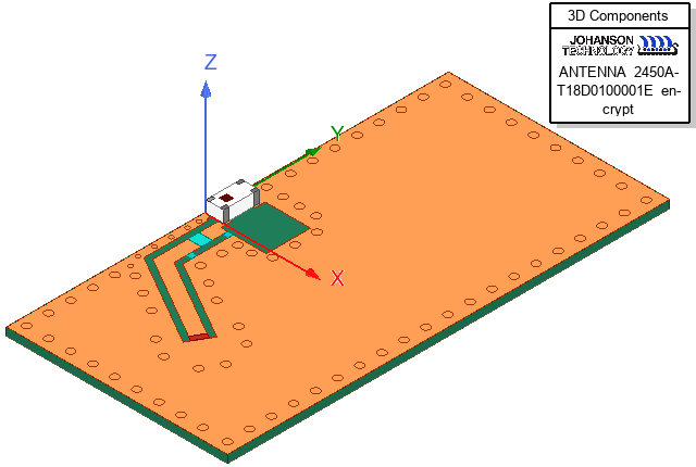
The antenna is designed to work at a frequency in the range of 2.4 to 2.48 GHz. The following images shows the evaluation board with the chip antenna mounted to it:
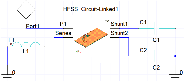
The next image shows the linked HFSS evaluation board along with its matching network circuit: