Assigning Anisotropic Impedance Boundaries
Planar screens or grids of large extent with periodic geometry can be replaced by an Anisotropic impedance boundary. The boundary applies a homogeneous characteristic impedance to the surface in an effort to create an equivalent electrical representation of the geometric grid pattern. For legacy designs, this boundary replaces the Screening Impedance boundary.
To assign an Anisotropic Impedance boundary
- Select a surface
on which to assign the boundary and click HFSS>Boundaries>Assign>Anisotropic Impedance
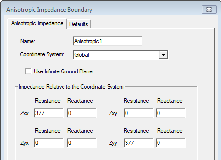
to bring up the Anisotropic Impedance
Boundary dialog.
- The Coordinate System drop-down menu lists the Global
Coordinate system and any relative coordinate systems if you have defined
them in the design. Select the Coordinate System that defines the anisotropic
characteristic of the impedance boundary. (See Creating a Relative
Coordinate System.)
Note:
An anisotropic boundary must not touch ports in a design.
- Select Infinite Ground Plane if you want the surface to represent an electrically large ground plane when the radiated fields are calculated during post processing.
- In the Impedance Relative to the Coordinate System area, you set the Resistance and Reactance. If Anisotropic Impedance is checked, the wizard shows Resistance and Reactance fields for X Axis alignment and Y axis alignment. These values can be numeric or can reference variables, including spatial variables x, y, and z. Isotropy will be inferred if Zxy and Zyx are left as zero.