
Adding an HFSS-PI Solution Setup
HFSS‑PI is a simulation workflow and solver technology for power‑integrity (PI) analysis that uses prism‑based meshing to efficiently handle complex on‑chip, interposer, and package‑level designs. It supports optional geometry simplification, such as reducing stackups, vias, and other primitives, to enable high‑efficiency simulation, and it leverages large‑scale high‑performance computing (HPC) resources for faster and more accurate results.
Setting Up an HFSS-PI Simulation
Follow these steps to add a HFSS-PI solution setup to a project in.
-
Open the HFSSPI1 window. There are several ways. For example:
- From the Simulation tab, click SIwave-PSI.
- From the Project Manager window, expand the Project Tree > [Active Design Folder]. Then right-click EMDesign1 or Analysis and select Add HFSS-PI Solution Setup.
- From HFSS 3D Layout, select Solution Setup > select Add HFSS-PI Solution Setup.
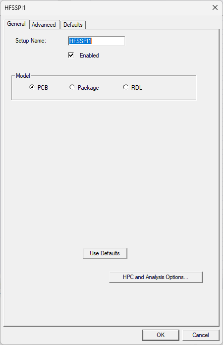
- From the General tab, set the following:
- Setup Name – type a name in the field or accept the default.
- Enabled – check the box to activate the setup.
-
Model Type – select PCB, Package, or RDL.
-
PCB – for full board layout.
-
Package – for physical enclosure and interconnects.
-
RDL – for integrated circuit or interposer-level analysis.
-
-
HPC and Analysis Options – open a window allowing you to specify HPC options
-
Use Defaults – undo any configuration changes and restore defaults.
- Click the Advanced tab.
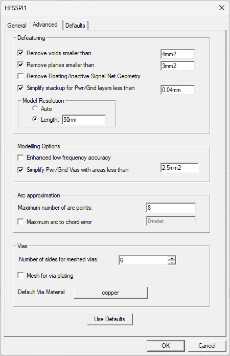
- From the Advanced tab, set the following:
- Remove voids with an area smaller than – check the box and enter a <value> to simplify meshing by removing small voids.
- Remove Floating/Inactive Signal Net Geometry – check the box to remove floating and inactive signal net geometry.
- Simplify stackup for Pwr/Gnd layers less than – check the box, enter a <value>, and metal layers with a thickness less than the specified value are set to 0 during simulation. The corresponding layer elevations are adjusted.
- Model Resolution – select Auto to automatically set the model resolution based on the design's geometry (recommended for most designs) or select Length to manually set a resolution threshold. Features smaller than the entered value may be merged with nearby geometry, snapped, or removed entirely, especially if they don’t affect the overall structure or function of the design (recommended if the design includes fine or critical details).
- Modeling Options:
- Enhanced low frequency accuracy – check the box to increase simulation accuracy at low frequencies.
- Simplify Pwr/Gnd Vias with areas less than – check the box to increase accuracy by removing vias smaller than the specified area threshold.
- Arc Approximation:
- Maximum number of arc points – the maximum number of mesh points on a given arc segment.
- Maximum arc to chord error – check the box and enter a value for the maximum distance permissible between a straight edge approximation (the chord) and the original arc.
- Vias:
- Number of sides for mesh vias – number of sides to use when creating the 3D representation. If less than 3, the via is modeled as a flat ribbon.
- Mesh for via plating – check the box to create a mesh around the plating percent specified in the Edit Padstack Definition window, resulting in a more accurate DC thickness value. A via that is not fully plated includes a void filled with the material defined in the surrounding air box (e.g., air). Zero plating is not recognized and is treated as fully plated.
Default Via Material – when a material has not been specified in the padstack definition and there is no override in the properties for a via, then this is the material associated with the via mesh. It is initially set to copper.
- Click the Defaults tab.
-
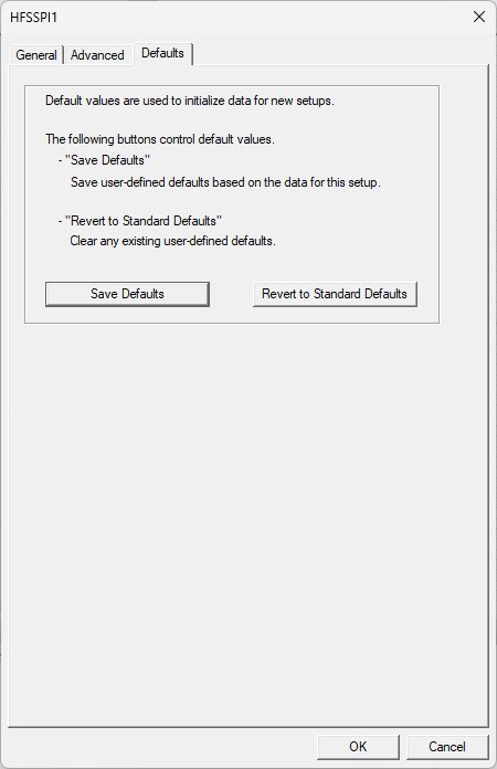
From the Defaults tab, set the following:
- Save Defaults – click to save user-defined defaults based on the data for this setup for all tabs.
- Revert to Standard Defaults – click to clear any existing user-defined defaults for all tabs.
- Click OK to add the HFSS-PI solution setup to the active design and simultaneously open the Edit Frequency Sweep window.
- From the Edit Frequency Sweep window, click OK to accept the sweep with its default values or change the default values before continuing. Refer to Adding a Frequency Sweep for more information.
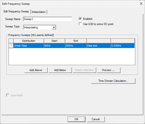
An enhanced interpolating sweep (i.e., enhanced PI sweep) is available for power integrity (PI) applications that require greater accuracy at low frequencies. This enhanced option is supported in both HFSS and HFSS‑PI simulation setups. This enhancement is a beta feature. Beta features must be activated prior to use. Refer to Activating the Enhanced PI Sweep Beta Feature for instructions.
Analyzing the Design
To run an HFSS-PI solution setup, navigate to the Project Manager window, right-click Analysis and select Analyze. Refer to Running Simulations.
Post-Processing with HFSS-PI Simulation Setups
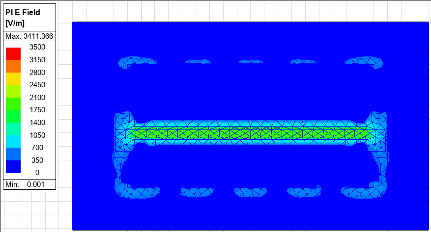
Complete these steps to plot a field overlay on the design.
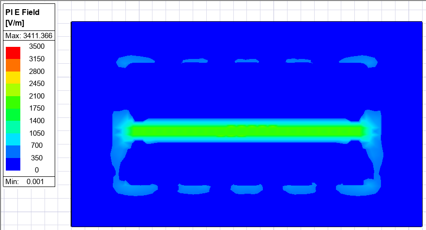
HFSS‑PI field plotting differs from the HFSS tetrahedral solver. E‑ and H‑field quantities are available only at specific XY elevations defined by the solver, rather than on user‑selected nets or stackup layers. Field overlays are therefore generated as XY cross‑sections at signal‑layer or clip‑plane elevations, not as surface‑based plots tied to geometry objects.
-
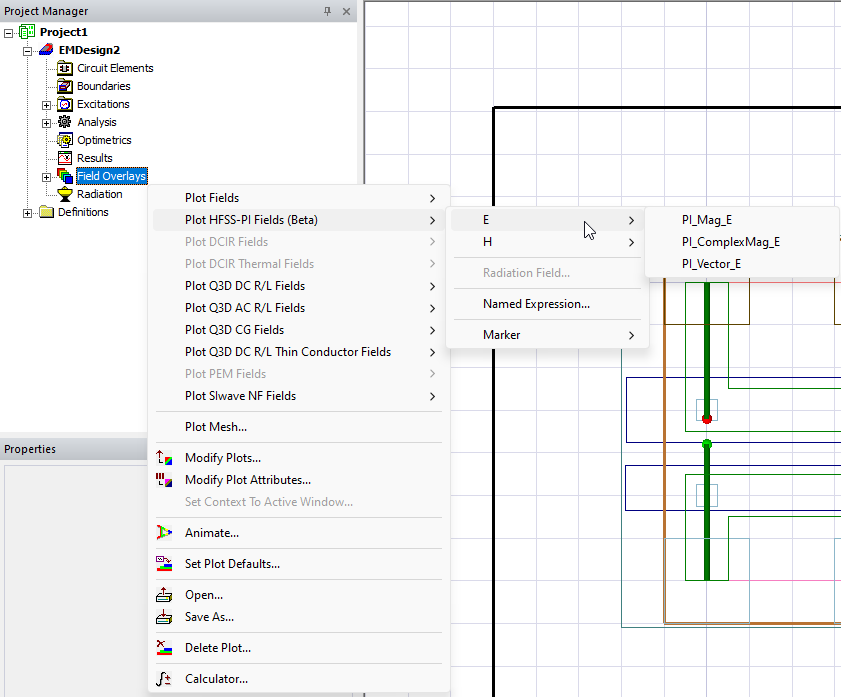
From the Project Manager window, right-click Field Overlays to view the available plot types. HFSS‑PI solution setups provide plot types unique to the PRISM solver workflow (i.e., PI_Mag_E, PI_ComplexMag_E, PI_Vector_E, PI_Mag_H, PI_ComplexMag_H, and PI_Vector_H). These quantities support XY cross‑section overlays for E‑ and H‑fields. Refer to Field Quantities.
-
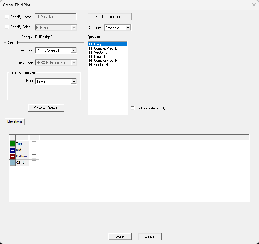
Select a plot type to open the Create Field Plot window.
-
Specify a Name, Folder, and adjust the default settings in the Context area. From the Quantity list, choose one of the HFSS‑PI field quantities (E‑field or H‑field). Then select one or more Layers from the Elevations table to define the XY cross‑section to plot. Refer to Plotting Field Overlays.
-
Click Done to create the field plot.
-
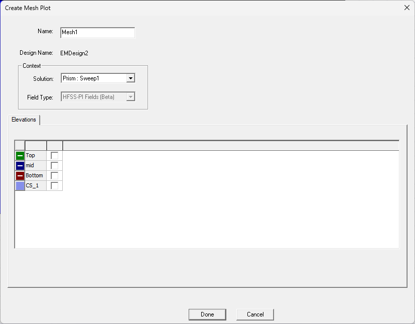
From the Project Manager window, right-click Field Overlays and select Plot Mesh to open the Create Mesh Plot window.
-
Select an HFSS‑PI solution from the Solution drop‑down menu to populate the Field Type list with PRISM‑solver‑specific mesh options. Then select one or more Layers from the Elevations table. Refer to Create Mesh Plot.
-
Click Done to create the plot mesh.
Activating the Enhanced PI Sweep Beta Feature
Follow these steps to enable the enhanced PI sweep.
-
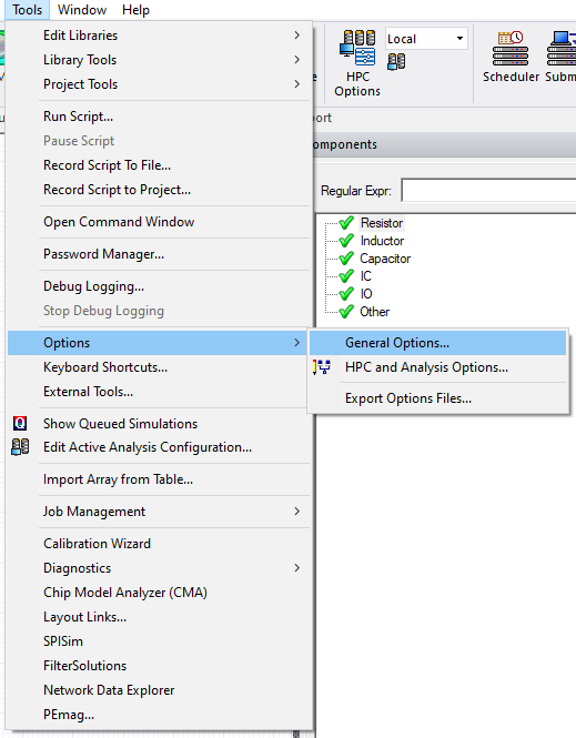
From the Tools menu, select Options > General Options to open the Options window
-
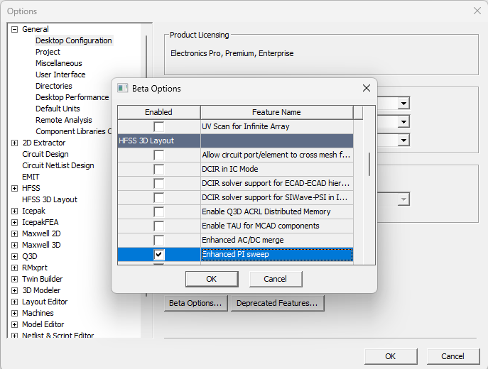
Expand General > Desktop Configuration and click Beta Options to open the Beta Options window
-
Scroll down to the HFSS 3D Layout section and check the box adjacent to Enhanced PI Sweep.
-
Click OK to close the Beta Options window.
-
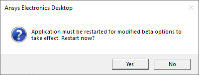
Click OK to close the Options window and open a prompt to restart the software. Users may be asked to save their work.
-
Click Yes to restart immediately.
-
After restarting the software, the enhanced PI sweep will be activated. There will be no visual UI change.
The procedure is complete.