
Structural Example – Substrate Warpage
This project determines the warpage of a semiconductor substrate and the printed circuit board (PCB) on which it is mounted. The PCB substrate, and solder objects are at an assumed uniform temperature of 120° C. The environment temperature (at which the model is stress free) is 20° C. Therefore, expansion is based on a ΔT of 100° C. The device has 90 pins arranged in a grid. The analysis looks at the equivalent stresses in all parts and particularly in the solder connecting the PCB and substrate.
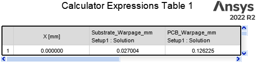
Since the displacement magnitudes are dominated by elongation and lateral expansion of the parts, two calculator expressions and two face selections have been defined to provide a warpage indication. Specifically, the Z-displacement (normal direction of the substrate and PCB planes) is the best indication of warpage. The calculator expressions determine the difference between the minimum and maximum Z-displacements for the top face of the PCB and the bottom face of the substrate, which are passed to the field calculator as face selections. A data table report is also defined to tabulate the two warpage indicators (in millimeters).
An imprinting operation has been used to create a total of four very small rectangular subfaces at three different corners of the PCB. These small faces provide a means of physically constraining the model (eliminating rigid body motion to make it statically stable). At the same time, constraints were able to be assigned in a manner that neither inhibited the thermal expansion and warpage of the model nor generated any local stress exaggerations.
The model has the following characteristics:
- Filename and Path (relative to the Examples folder of the program installation):
- Number of Parts: 92 solids
- PCB: Consists of the circuit board substate only, without copper traces
- Substrate: The substrate of a very large-scale integration (VLSI) semiconductor
- Solder1 through Solder90: Interconnecting solder grid between the PCB and substrate, with each one a cylindrical object
- Materials:
- FR-4: PCB dielectric
- silicon: Semiconductor Substrate
- Solder Eutectic Sn-37Pb: All Solder objects
- Mesh Operations: No mesh operations; default initial mesh settings
- Boundaries:
- FixedSupport1 (at small imprinted subface at +X, -Y corner of the PCB)
- FrictionlessSupport1 (at small imprinted subface at +X, +Y corner of the PCB, bottom side)
- FrictionlessSupport2 (at small imprinted subface at +X, +Y corner of the PCB, front side)
- FrictionlessSupport3 (at small imprinted subface at -X, +Y corner of the PCB, bottom side)
- Excitation:
- ThermalCondition1: Uniform, all objects, 120° C (stress-free Environment Temperature is 20° C)
- Results:
- Calculator Expression Table 1: PCB_Warpage_mm and Substrate_Warpage_mm (ΔDz in millimeters at top face of PCB and bottom face of Substrate, respectively)
- Design Table 1: Volume of Q1 body and terminals, with total
- Field Overlays:
- Mesh1 (undeformed): Mesh plot assigned to all objects
- Mesh2 (undeformed): Mesh plot assigned to solder objects
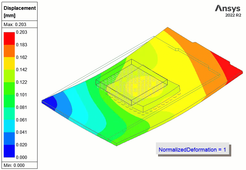
- Mag_Displacement1 (scaled deformation): Displacement overlay assigned to all objects; animation defined
- Equivalent Stress1 (undeformed): Stress overlay assigned to all objects
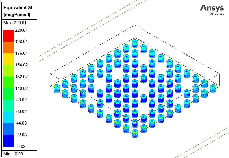
- Equivalent Stress2 (undeformed): Stress overlay assigned to solder objects
Mechanical\Structural\SubstrateWarpage.aedt
The solid objects are grouped by components and materials, as follows:
The initial mesh slider has been enhanced to produce suitable thermal and structural solution meshes with minimal usage of manually defined mesh operations. Both flat and curved faces are now refined by this slider for these two solution types. In earlier versions of the software, mesh operations would have been required to produce a high-quality mesh at the critical solder objects and the areas near the solder contact points on adjacent parts. Now, the default position of the Initial Mesh Settings slider produces acceptable results.
The following image is the Calculator Expression Table showing derived warpage values:
The following animation is the displacement magnitude overlay:
The following image is the equivalent stress overlay assigned only to the solder objects:
- The warpage of the PCB and Substrate are approximately 62.2% and 13.3% of the peak displacement magnitude, respectively.
- The maximum equivalent stress in the solder is well above the yield strength of the material, which is approximately 43 MPa. As such, all values above 43 MPa are invalid as they assume a constant Young's Modulus. In reality, the slope of the stress-strain curve decreases beyond yield, and further strain increases the stress at a much lower rate. The ultimate tensile strength of the material is 52 MPa, and breakage occurs at around 32% elongation.
- The above-yield stresses are localized at the edges of the top faces of the solder objects, particularly those along the perimeter of the solder grid. A significant portion of each solder/substrate contact face remains below the yield strength of the material.
- Solder is prone to creep at relatively low temperatures and stresses, which tends to relieve stresses in solder connections. Considering this characteristic and the high amount of elongation the material can survive, the solder objects will likely not fail despite the localized high stresses that were calculated.