Setting Up an SVPWM Excitation
Pulse Width Modulation (PWM) is a term used for any method that produces a square wave signal with varying duty cycle and frequency to control the average power delivered to a load. PWM is widely used in applications such as light dimming, switching power supplies, and electric motor drive. In these types of designs, the AC motor needs to be powered by an alternating current excitation, which is supplied by the DC supply voltage through an inverter circuit using power device switches. Controlling how the power switches are turned on and off is accomplished by PWM.
For 3D and 2D magnetic transient T-Omega solutions, Space Vector Pulse Width Modulation (SVPWM) can be directly created in Maxwell for three-phase voltage-excited windings. For all three phases, Maxwell will calculate the PWM voltage waveforms based on user inputs and automatically set up the winding excitations in the transient simulations. The generated waveform represents the Phase-Neutral voltage, and it is applicable to Y(star)- or delta-connected winding.
- Before setting up the SVPWM excitation:
- Define three PWM voltage windings. For the Type option in the Winding window, make sure to select PWM Voltage:
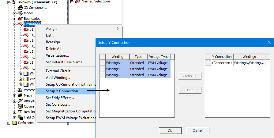
- If you will be using a Y connection for the winding, right click on the Excitations entry in the Project Manager, and select Setup Y Connection. Select the three windings, and click Group.
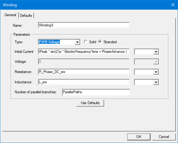
Note that when the PWM Voltage type is selected, the Voltage field is grayed out because it will use the data generated by PWM voltage excitation setup.
- For 3D transient designs, only stranded windings are allowed for the Y-connection.
- For 2D transient designs, both stranded and solid windings are supported, but a mix of stranded winding and solid winding in one Y-connection group is not allowed.
- A mix of PWM voltage winding and (normal) voltage winding in one Y-connection group is not allowed.
- Only one Y Connection is allowed in a given Maxwell design.
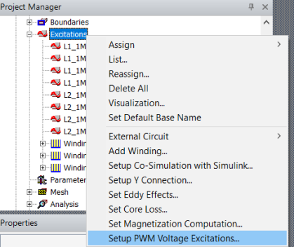
- In the Project Manager tree, right click Excitations, and select Setup PWM Voltage Excitations.
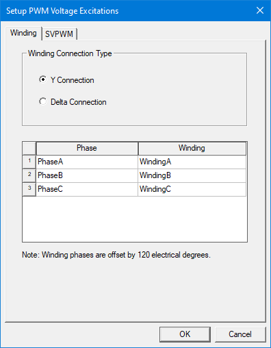
- In the Setup PWM Voltage Excitations window that opens, select either the Y Connection or the Delta Connection, and arrange the three windings to represent the three phase windings (PhaseA, PhaseB and PhaseC) accordingly. Note that the Winding drop-down menu will only include windings that were defined as the PWM Voltage type.
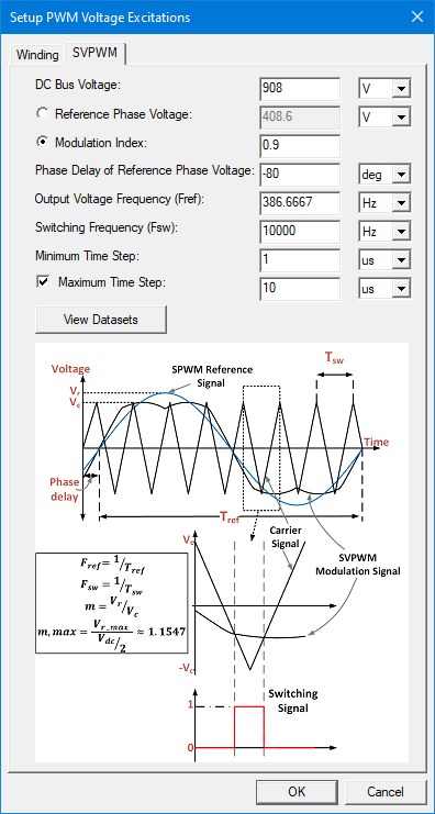
- Click on the SVPWM tab, and input the corresponding parameters for SVPWM. Example parameters are shown below:
- DC Bus Voltage – Specifies the voltage available at the main DC bus as input to the inverter.
- Reference Phase Voltage – Defines the reference voltage signal, seen as the blue curve (labeled SVPWM Reference Signal) in the diagram in the Setup PWM Voltage Excitations window. If this option is selected, the Modulation Index setting is grayed out and automatically calculated according to ModulationIndex = ReferencePhaseVoltage/(DCBusVoltage/2).
- Modulation Index (m) – Specifies the ratio between the reference signal to the carrier signal; it determines the amplitude of the fundamental output voltage with respect to the available DC bus voltage as described by the equation below.

The range of the modulation index is 0 < modulation index ≤ 2/sqrt(3) (i.e., approx. 1.1547) for SVPWM.
Important: For a small modulation index, care must be taken when setting the minimum time step to control numerical error.If this option is selected, the Reference Phase Voltage setting is grayed out and automatically calculated according to ReferencePhaseVoltage = ModulationIndex*(DCBusVoltage/2).
To understand how the maximum modulation index is calculated, start with the figure below, which shows the space vector hexagon (represented by six sectors and eight vectors). Each vector represents a different switching state of the inverter.
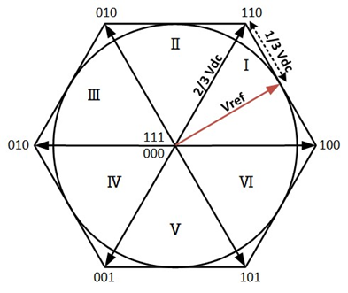
The vector Vref is the reference revolving voltage vector formed from the three phase sinusoidal voltages; at each sector, this vector is realized by alternating between the two nearest space vectors along with the zero vectors.
The circle inside the hexagon represents the maximum value possible for Vref (and hence the output voltage) that can be produced with the SVPWM technique.
Knowing that the magnitude of each vector is 2/3 VDC, the maximum value of the output voltage (Vref) can be computed as


From these definitions, the maximum modulation for SVPWM can be derived as

- Output Voltage Frequency (Fref) – Defines the fundamental frequency of the reference signal, and therefore, the PWM output voltage.
- Switching Frequency (Fsw) – Defines the carrier signal frequency that is used to generate the PWM switching signal. A typical value for traction inverters is between 10 – 20 kHz.
- Phase Delay – Defines the phase delay angle of the reference signal (and hence the output voltage). The phase delay depends on the operating point, and it can be provided from system-level simulation or by running a transient simulation with an ideal sinusoidal current and checking the phase delay on the output of the phase voltage.
- Minimum Time Step – Defines the rate at which the carrier signal and the reference signal are compared to generate the switching signals. This value is important to correctly capture the switching events. The recommended value is 1/(Fsw*100) or smaller.
- Maximum Time Step – Optional setting that specifies the largest time step that can be used to generate the switching signal; it is used to modify the time step dataset; see the explanation that follows. If left unchecked, there will be no maximum time step considered when the time step dataset is created. If checked, the default value is 10*Minimum Time Step.
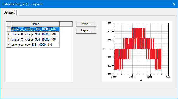
- View Datasets – Click to view the new datasets generated by the PMW Voltage Excitation setup.
- Click OK.
Alternatively, from the menu bar, select Maxwell 2D/3D > Excitations > Setup PWM Voltage Excitations.
Three datasets of the voltage (Phase_X_voltage_<Fref>_<Fsw>) vs. time are generated based on the settings. The datasets are generated by comparing the reference signal to the triangular carrier at a sampling frequency defined by the minimum time step. Subsequently, the datasets are reduced by removing the timesteps where no change of the voltage values occurs.
The datasets represent the three normalized PWM phase voltages for one electrical cycle. The phase sequence of the generated dataset is A-B-C with Phase B and C lagging Phase A with 120 deg and 240 deg, respectively. If a variable was used to define a setting, the View Dataset function will only display nominal values.
A time step dataset is also created. Note that when creating the time step dataset, the solver considers the Maximum Time Step (dt), and it will add N more time steps (equal spaced) between the two time stamps Y(n-1) and Y(n) (say deltaT = Y(n) - Y(n-1)) when deltaT > dt, and N = floor(deltaT/dt). For example, with timeStep = [1.7, 2, 3.3] and dt = 0.4, then newTimeStep = [1.7, 2, 2.325, 2.65, 2.975, 3.3]. Three new time steps are added: 2.325, 2.65, and 2.975, and they are equally spaced between 2 and 3.3.
The technique used by the Maxwell application to implement SVPWM excitation computes the pattern of voltage pulses for each of the three datasets by comparing a triangular carrier wave with frequency Fsw and amplitude 1 to three reference functions.
Unlike for sinusoidal PWM, where the reference functions are sinusoidal, for this SVPWM implementation, the three reference functions (Va_Ref, Vb_Ref, Vc_Ref) need to be constructed as a first step. This is achieved by superposing the common mode voltage (VCM) to the three sinusoidal signals (Va_0, Vb_0, Vc_0) of a three-phase system:
Va_Ref = Va_0 + VCM
Vb_Ref = Vb_0 + VCM
Vc_Ref = Vc_0 + VCM
Va_0 is defined as ModulationIndex*sin(2*pi*Fref*time-Phase Delay). Vb_0 and Vc_0 lag Va_0 by 120° and 240°, respectively.
The amplitude Vmax can be calculated as (DC Bus Voltage)/2 * Modulation Index.
At every timestep, the common mode voltage is calculated as half of the mid-valued function among Va_0, Vb_0, Vc_0.
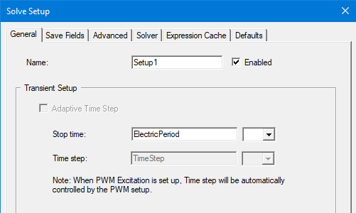
The dataset time_step_size_<Fref>_<Fsw> tracks the exact instance the switching happens and will be used to define the variable time step in the transient setup to ensure that all switching events are captured with the minimum number of time steps possible. This dataset will be used in the Solve Setup Time step value field, so the Time step value field is grayed out. For a 2D analysis, the Adaptive Time Step check box is grayed out as well.