
HFSS 3D Layout Getting Started Guides
The following guides are tutorials covering various types of HFSS 3D Layout designs. These Getting Started guides typically walk you through the steps to build the geometry, set up the solution, run the analysis, and evaluate the results (by generating plots, overlays, and animations):
This Getting Started guide describes a low pass filter model. It includes instructions to create, solve, and evaluate the results of a low pass filterusing the HFSS 3D Layout design type in the Ansys Electronics Desktop application.

This Getting Started guide describes a microstripfilter model. It includes instructions to create, solve, and analyze the results of a microstrip filter using the HFSS 3D Layout design type in the Ansys Electronics Desktop application.

Inserting an HFSS 3D Layout Design
Now that the application is launched and a new project has been automatically added and named, complete these steps to insert an HFSS 3D Layout design.
- From the Desktop ribbon, select HFSS 3D Layout from the HFSS drop-down menu.
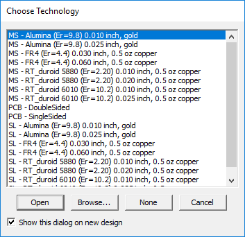
- If the Choose Technology window opens, click None to open the Layout Editor.
 Note:
Note:- All EM designs must define a process topology (also called a stackup).
- Layout technology files provide a quick way to store frequently used process topologies (e.g., an engineer who frequently uses a specific substrate can pre-specify the correct materials and stackups with a single click).
- This example does not use a layout technology file. The topology or stackup is manually defined.
- Optionally, hide the Message Manager and Progress windows if either is currently displayed.
- From the View menu, deselect the check-boxes for Message Manager and Progress.
- Alternatively, click Hide Messages and Hide Progress along the bottom of the program window.
A list of example projects included with the HFSS 3D Layout installation is located here.