
De-embedding of Design Under Test from Test Fixture
This section describes de-embedding, that is the impact of the test fixture on the measurement result is removed from the measurement data thereby allowing characterization of the device under test (DUT). This is accomplished by means of:
- Custom Calibration Kit
- YZ De-embedding
- Modeling and Simulation
- Automatic Fixture Removal (AFR)
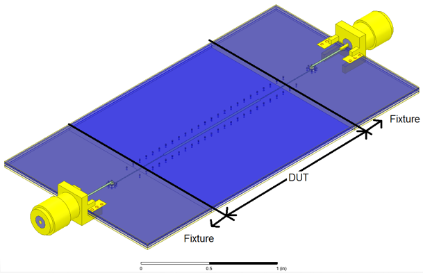
Illustration of Fixture and Device Under Test (DUT)
The total structure includes the following:
- CAD drawing of the Fixtures and Device Under Test (DUT)
- We want the response of just the DUT, but we can only measure at coaxial connectors.
- Notice that the Fixtures are identical. While not necessary, this makes the de-embedding a little easier.
De-embedding: Custom Calibration
This section describes how you can make a calibration kit on your PCB. In this case, we use Short-Open-Load-Thru (SOLT). You can also use a variant called Short-Open-Load-Reciprocal (SOLR), sometimes called Short, Open, Load, Unknown Thru. The process needs well-defined standards which can be difficult to get at high frequency.
We also use a technique called Use Multiline Thru-Reflect-Line (TRL) described in Reference [3].
- Use multiple Lines to get required bandwidth as each line can only cover a line whose electrical length is between 200 and 1600
- Used by National Institute of Standards and Technology (NIST)
- Can take a lot of space to get lines long enough for low frequency measurements
While there are many other calibration methods, with well defined standards, this is an excellent choice. It can be difficult to make, and characterize, standards at a necessary reference plane.
De-Embedding: YZ De-embedding Described in Reference [4]
This approach is used mainly for on-die (i.e. on-wafer) measurements.
- Measure an Open Standard (i.e. the Y-standard)
- Measure a Short Standard (i.e. the Z-standard)
- Convert the measured device, with fixture, to Y-parameters and subtract Y-parameters of Open. Call this YYremove. Also, remove the open standard from the Z-standard.
- Convert YYremove to Z-parameters and subtract the Z-parameters of the Y-corrected Short Standard. The result is the de-embedded DUT.
- Assumes that the Fixture is electrically small.
- Easy to have electrically small structure on-die, but harder to do on PCB.
De-embedding: Modeling and Simulation
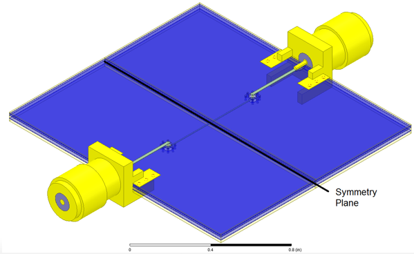
To perform the de-embeding for Automatic Fixture Removal (AFR as described in Reference [5]):
- Concatenate the Fixture.
- Make symmetric (as this is much easier).
- Measure 2X Thru. Use this structure
- Create circuit model of each fixture half and concatenate as well
- Use Lumped Element
- Or Distributed
- Match of model to measurement must be excellent, or you will introduce error
- Simulate with full-wave solver like HFSS.
- You need to know surface roughness, dielectric properties, etc.
- Match in S-parameters needs to be excellent, or you will introduce error.
Using Signal Flow Graphs (see References [6, 7]), we can model the 2X Thru.
- Notice the S-parameters in each half.
- 2X Thru has symmetry. Also, S21=S12 since they are reciprocal.
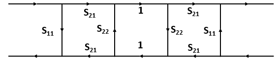
These are the S-parameters we are looking for, but we are measuring the 2X Thru, so we only know:
- S11,2X_THRU=S22,2X_THRU=S11 since symmetric
- S12,2X_THRU=S21,2X_THRU=S21 since reciprocal
So, solve these equations
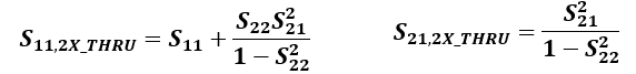
This gives us two equations with three unknowns.
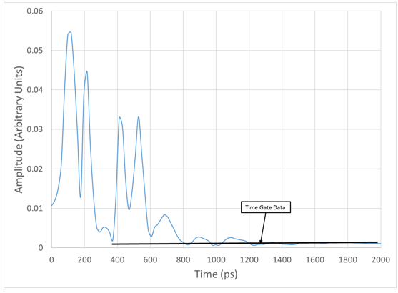
Use time gating to learn S11.
- Take inverse Fourier Transform of S11,2X_THRU
- At half-way point in time, set level to that of a matched termination.
- Take Fourier Transform of gated data
- This is S11 of the Signal Flow Graph
- Now you have two equations and two unknowns to find S21 and S22
- Recall square root of complex number is (in mag/ang format):
- √Magnitude∠ᶿ⁄2
Solving is outside the scope of this chapter, but once solved you have the fixtures.
With S-parameters of the fixture
- Use ABCD parameters described in Reference [6] to remove fixture effects from measured data to get DUT
- Can use T-parameters described in Reference [7] as well.
- Or, use Nexxim with Reciprocal option to de-embed the data for you.
Next
Example of Determining PCB Material Properties: Q2D and Nexxim to HFSS