Layout Window
The Layout Window is a dockable Ansys Electronics Desktop window that can be resized and relocated, and can be used to view and configure various layout settings. Use the right-click menu of the Layout Window to configure the following:
- Set Active – makes the current layer the active layer.
- Show This Layer Only – makes the current layer the only visible layer.
- Show All Dielectrics – makes all Dielectric layers visible.
- Hide All Dielectrics – makes all Dielectric layers invisible.
- Show All Signals – makes all Signal layers visible.
- Hide All Signals – makes all Signal layers invisible.
Use the Layout window to alter the following controls for setting visibility by layout-object type.
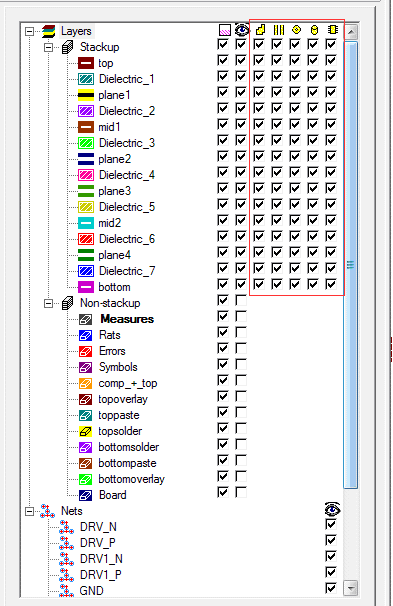
The following controls are available:

|
Controls the visibility of shapes |

|
Controls the visibility of lines (paths) |

|
Controls the visibility of pads |

|
Controls the visibility of holes |

|
Controls the visibility of components |
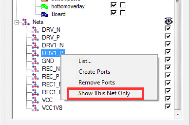
You can also turn visibility off for all nets but the selected net by right-clicking and selecting Show This Net Only.