
Johanson 2450AT18D0100-EB1SMA
Abstract
This example is one of two Johanson Technology chip antenna and evaluation board (EVB) models that you can find in the Examples\HFSS\Antennas subfolder included in the Ansys Electromagnetics Suite installation. Additionally, this model is associated with the following HFSS Getting Started guide:
Getting Started with HFSS: Matching Network – Using Tuning in Circuits
The geometry is identical between the example model and getting started guide. The project filenames differ between the two. The example model shows how to tune a matching network automatically using optimization analyses. By contrast, the getting started guide shows how to tune the matching network's component values manually in a Circuit design and push the resultant excitations to the HFSS design.
This example demonstrates the following:
- Using Johanson 3D Components
- Using lumped components to match the antenna (optimizing its performance)
- Optimizing the matching network automatically and entirely within HFSS
- Dynamically linking an HFSS design to a Circuit simulation for optimizing a matching network
- Generating several types of plots and overlays
Simulation Time (Intel Xeon Gold, 2.9 GHz, 16 cores, 8 variations in parallel, version 2025 R2):
- HFSSDesign1:
- Adaptive solution and sweep – 5m : 16s, 3.84 GB Maximum memory/process
- Optimization – 1m : 49s
- Matching_Network (Circuit):
- Linear frequency sweep – 2 seconds
- Optimization – 7 seconds
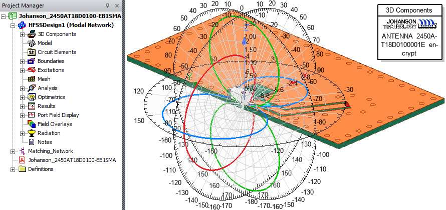
Figure 1: Johanson Chip Antenna and EVB with Overlaid 2D Gain Plots
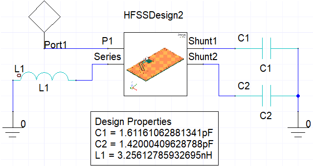
Figure 2: Matching Circuit Schematic
Model and Setup Details
The model consists of a single chip antenna mounted to an EVB – Johanson Technology, legacy part number: 250AT18D0100-EB1SMA. The antenna is a vendor model included as an encrypted 3D component. It is excited by a lumped port and contained within an automatically defined open region with a radiation boundary, as detailed below.
The example project contains two designs, summarized as follows:
- HFSSDesign1 (Modal Network): In this design, tuning components are represented as lumped port excitations with renormalized impedances and variable capacitance and inductance values. When the optimization setup is solved, the tuning component values are adjusted to achieve two goals: a realized gain of at least 2.5 dB and a return loss no greater than -40dB at 2.44 GHz.
- Matching_Network: A Circuit design that is dynamically linked to HFSSDesign1. In this case, the optimization is based solely on the goal of achieving a return loss no greater than -40 dB. As an alternative to optimization entirely within HFSS, you can save the optimized network parameters in the Circuit design and push the revised excitations to the linked HFSS design. In this example, we show you the Circuit optimization setup and the resulting S11 parameter versus frequency. However, the matching network component values used for the reports in HFSSDesign1 are the ones determined by the optimization setup in HFSSDesign1.
In addition to the automatic optimization shown in this example model, Circuit Optimetrics also allow you to tune a matching network by manually varying component values using sliders. You can immediately see the effect on the results when you change a slider position. To access this feature, right-click Optimetrics in the Project Manager (in the Matching_Network branch) and choose Tuning from the shortcut menu. See the related Matching Network getting start guide, referenced in the previous Abstract section. It provides step-by-step instructions on the manual tuning process and pushing the excitations from the tuned circuit design to HFSS.
As an alternative approach to circuit tuning, you can substitute postprocessing variables for the renormalized impedance values. By varying the postprocessing variables, you can immediately see the effect on the design behavior (without having to rerun the solution). Similarly, you could scale the field amplitudes in the Edit Sources dialog box to see immediate tuning results.
This topic describes the setup of the HFSSDesign1 antenna evaluation board solution and its results, including the optimization setup. It also describes the linear frequency sweep and optimization setups in the Circuit design (Matching_Network). For details concerning adding lumped components for tuning, see Assign Lumped Ports for Modal Solutions.
For both designs, the tuning component values are set at the following initial values:
C1 = 2 pF, C2 = 1.5 pF, L1 = 3.5 nH
In order to ensure that the optimization analyses in both designs start with these values, be sure to solve the analyses in the following order:
- Solve HFSSDesign1 > Analysis > Bluetooth
- Solve Matching_Network > Analysis > LinearFrequency
- Open Matching_Network > Results > S Parameter Plot1 (return loss)
- Solve Matching_Network > Optimetrics > neg40dB_ReturnLoss
- Solve HFSSDesign1 > Optimetrics > RealizedGain_and_S11
Observe the return loss based on the initial component values. Leave this plot open as you preform the next step to see the effects of the component optimization iterations in real time.
Observe the optimized tuning component values, but do not copy them or push the excitations to HFSSDesign1.
HFSSDesign1 Details:
- Open Region: The Auto-Open Region option is selected in the Solution Type dialog box, and the type of region is Radiation.
- Boundaries:
- Finite Conductivity (FiniteCond1), 58 x 106 Siemens/m, classic infinite thickness model, at bottom face of PCB (HFSS > Boundaries > Assign > Finite Conductivity)
- Excitations:
- Lumped Port (P1), 50 Ω impedance, single mode, located at beginning of antenna feed. Renormalize All Modes and Deembed options selected, Port Renormalization Type = Impedance.
- Lumped Port (Series), 50 Ω impedance, Renormalize All Modes and Deembed options selected, Port Renormalization Type = RLC, Parallel, Inductance, value = L1.
- Lumped Port (Shunt1), 50 Ω impedance, Renormalize All Modes and Deembed options selected, Port Renormalization Type = RLC, Series, Capacitance, value = C1.
- Lumped Port (Shunt2), 50 Ω impedance, Renormalize All Modes and Deembed options selected, Port Renormalization Type = RLC, Series, Capacitance, value = C2, Deembed and Renormalize All Modes options selected.
- Mesh Settings:
- No mesh operations
- Initial Mesh Settings: The Curved Surface Meshing slider is set three ticks coarser than default. This setting only affects curved geometry, which is limited to the vias connecting the top and bottom ground planes for this example. The default curved surface resolution would be unnecessarily fine for these vias and would significantly increase the element count, solution time, and memory requirement.
- Analysis Setup:
- Bluetooth: The single solution frequency is 2440 MHz, 7 passes, Do Lambda Refinement is enabled, 30% max refinement per pass, Auto Select Direct/Iterative is selected, and Save Fields is enabled.
- 1_4GHz: 1–4 GHz sweep in 0.01 GHz steps, 250 maximum solutions, and 0.5% error tolerance
- Optimization Setup (RealizedGain_and_S11):
- Optimizer: Quasi Newton(Gradient)
- Goal 1: Peak Realized Gain ≥ 2.5 dB
- Goal 2: Return Loss ≤ -40 dB
- Acceptable Cost = 0, Noise = 0.0001
Sufficient local refinement is achieved in the area of the matching network due to the usage of lumped ports for the tuning components.
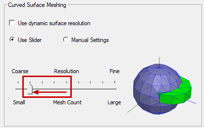
Figure 3: Initial Mesh Settings Dialog Box, Curved Surface Meshing Section
Maximum Delta S has been relaxed to 1. This setting is the maximum allowed change in magnitude between iterations, enforced for all S parameters. A separate expression is defined under the Expression Cache tab. The magnitude of S11 (the return loss at port P1) is specified with a convergence tolerance of 0.02. This technique provides a more efficient (faster) solution that focuses on the result of interest and allows a looser convergence tolerance for other results. The return loss is of interest because it is part of the basis of optimization that will be performed, and it is very sensitive to the tuning of the matching network.
Matching_Network (Circuit Design) Details:
- Analysis Setup (LinearFrequency): 1–4 GHz in 0.005 GHz increments
- Optimization Setup (neg40dB_S11):
- Optimizer: Quasi Newton(Gradient)
- Goal: Return Loss ≤ -40 dB
- Acceptable Cost = 0, Noise = 0.0001
Postprocessing
After solving (Simulation > Analyze all), you can view different post-processing results. Look in the Project Manager under Results and double-click on the different predefined reports (Figure 4):
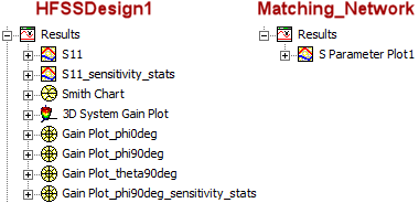
Figure 4: Predefined Reports Listed in the Project Manager
Predefined Reports – HFSSDesign1:
The following figures show the eight predefined reports in HFSSDesign1 along with some plot definition information. All results are based on the tuned matching network as solved by the HFSS RealizedGain_and_S11 optimization analysis.
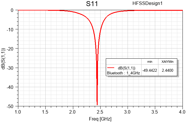
Figure 5: S11 – Return Loss (dB) after HFSS Optimization
Two of the predefined plots demonstrate sensitivity of the return loss and realized gain to small variations of the tuning component values. In the Families tab of the Report dialog box, C1, C2, and L1 were cleared from the Nominal Variables table. Then, the sweeps were edited to produce three representative variations of each value covering somewhere near a +/- 10% range relative to the optimized value.
Figure 6 shows the tuning component values used for both sensitivity statistics plots (Figure 7 and Figure 13) and how the variations were defined:
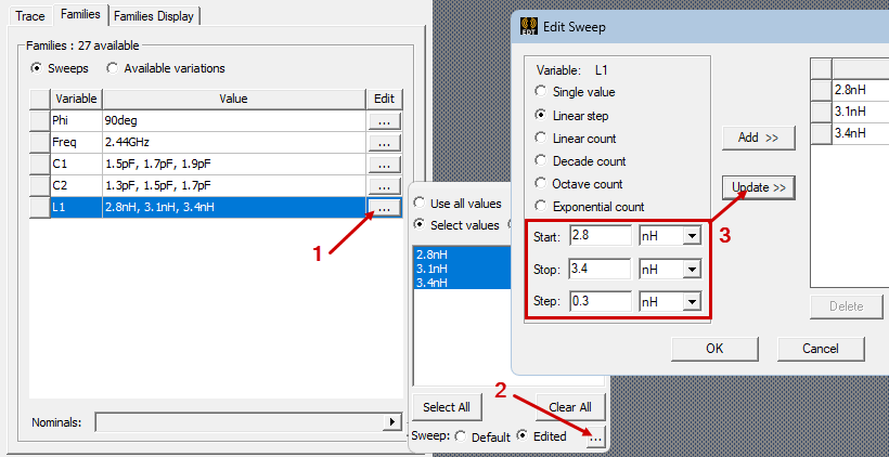
Figure 6: Defining Component Variations for Sensitivity Plots
The resulting 27 combinations of these component values are filtered down to three traces by the selection of Min, Max, and Avg under the Statistics option in the Families Display tab.
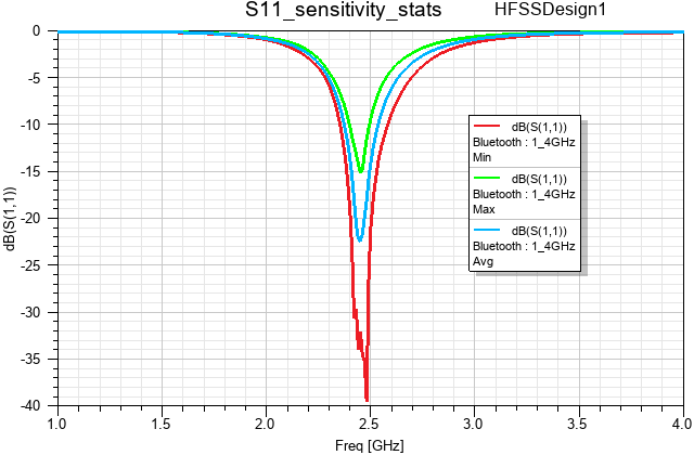
Figure 7: S11 – Return Loss – Sensitivity Statistics (dB)
The preceding plot shows that the return loss is very sensitive to a small change in the matching network tuning.
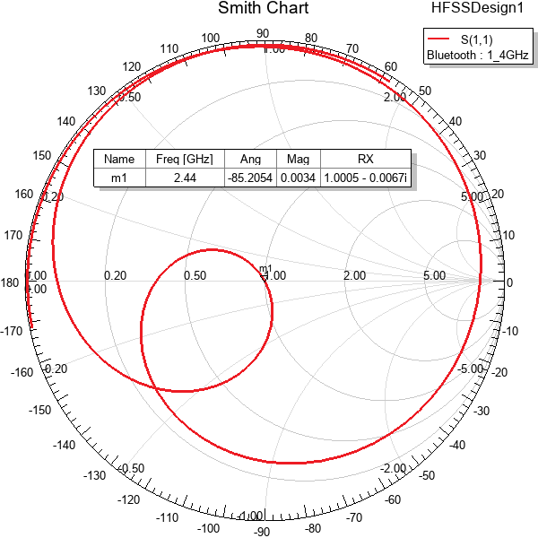
Figure 8: Smith Chart
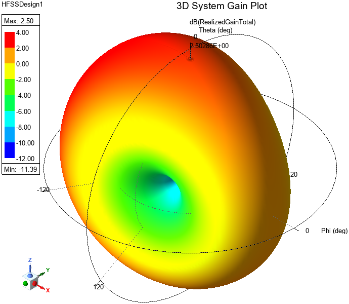
Figure 9: 3D Total Realized Gain (dB)
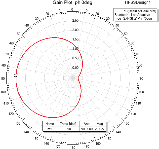
Figure 10: Total Realized Gain (dB) vs. Theta at Phi = 0°
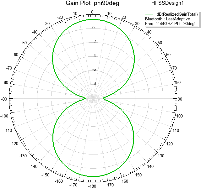
Figure 11: Total Realized Gain (dB) vs. Theta at Phi = 90°
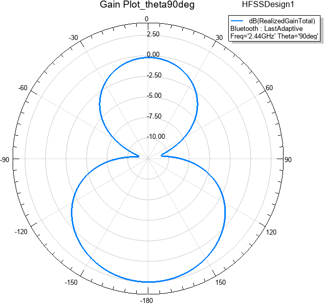
Figure 12: Gain Plot – Total Realized Gain (dB) vs. Phi at Theta = 90°
The Families definition of the following sensitivity plot is the same as shown in preceding Figure 6. The plotted quantity below is realized gain instead of return loss.
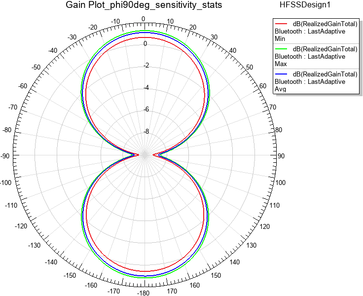
Figure 13: Gain Plot Sensitivity Statistics
The preceding plot shows that the gain is relatively insensitive to the matching network tuning as compared to the return loss.
Overlaying Reports on the Model Geometry:
To overlay any of the 2D or 3D gain plots on the model geometry, right-click in the Modeler window and choose Plot Fields > Radiation Field from the shortcut menu. In the Overlay Radiation Field dialog box that appears, select the checkbox in the Visible column for one or more of the available gain plots and click Apply. Adjust the Transparency or Scale as desired and click Apply again. Click Close when finished.
Figure 1, near the beginning of this topic, shows three 2D gain plots overlaid on the HFSS model geometry.
Predefined Report – Matching_Network (Circuit) Design:
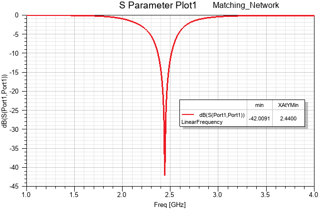
Figure 14: Return Loss versus Frequency (dB) after Circuit Optimization