
HFSS 3D Layout Stackup
FilterSolutions sets up the HFSS 3D Layout stack up and ports automatically in a efficient manner so as to maximize simulation efficiency and accuracy and to minimize manual user burden. Both single ports and dual ports are supported. Supported stack up configurations are listed in table 1 below:
|
Configuration |
Description |
Port Type |
|
Conductor equally spaced above and below a ground plate |
Wave Port |
|
|
Unbalanced Strip Line |
Conductor unequally spaced above and below a ground plate |
Wave Port |
|
Micro Strip |
Conductor placed above a dielectric layer and ground plate |
Lumped Port |
|
Micro Strip With Cover |
Conductor placed above a dielectric layer and ground plate and below an air pace with a ground plate |
Lumped Port |
|
Suspended Micro Strip |
Conductor place above a dielectric layer, airspace, and ground plate |
Lumped Port |
|
Suspended Micro Strip With Cover |
Conductor place above a dielectric layer, airspace, and ground plate and below an air pace with a ground plate |
Lumped Port (Unless symmetric) |
|
Inverted Micro Strip |
Conductor place above an airspace and ground plate, and below a dielectric layer |
Lumped Port |
|
Inverted Micro Strip With Cover |
Conductor place above an airspace and ground plate, and below a dielectric layer, air pace and ground plate |
Lumped Port (Unless symmetric) |
|
Conductor placed above and below a dielectric layer with air space above and below, and at least one ground plate |
Lumped Port (Unless symmetric) |
|
|
Symmetric Micro Strips |
Conductor above, below, or both placed above and/or below a dielectric with optional equally spaced air layers and required ground plates above and below the dielectric layer |
Wave Port |
Table 1: List of HFSS 3D Layout Stack Up Configurations
Setting up the Substrate In FilterSolutions
FilterQuick Panel
Click the substrate icon to bring up the Substrate Definition panel, as shown in Figure 1:
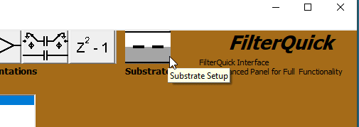
Figure 1: Selecting the FilterQuick Substrate Icon
The Substrate Definition panel will appear as shown below in Figure 2. Select the topology desired, layer dimensions, and materials, and then Close and Exit. Dielectric and conductance values may be entered with a numerical text entry, if desired. i.e., "4.56" for a dielectric constant or conductance of 4.56. Dielectric name may be entered with a name, colon, and number. For example, "MyDielectric:6.78" will create a dielectric name of "MyDielectric" and a dielectric constant of 6.78. At export time, HFSS 3D stack up is created in Overlap mode that conforms to the substrate definition.
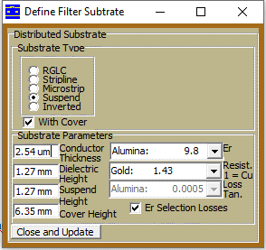
Figure 2; FilterQuick Substrate Definition Panel
Advanced Panel
Click the "Substrate" tab in the lower right of the Advanced panel, as shown in Figure 3 below. From there, substrate setup remains the same as described in FilterQuick above.
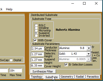
Figure 3: Advanced Panel Substrate Definition
HFSS 3D Layout Stack Up
An HFSS 3D Layout stack up is created in Overlap mode that matches the substrate definition. Overlap mode is advantageous in that it permits the addition of additional via layers, if the designer desires to add more parts to the HFSS 3D Layout design that require via layers.
Symmetric Substrates
Strip Lines are by definition symmetric. Micro strips may be made to be symmetric by selecting a suspended or inverted micros strip with cover, and with the cover height distance set to be equal to the suspended height distance. Symmetric substrates are assigned wave ports, just like strip lines.
Stack Up Vias
Nuhertz project via elements that attached to the lower and sometimes upper ground plate are included in all FilterSolutions project exports that contain such vias, including for suspended and inverted substrates. This via grounding through an air layer simulates properly, but the physical construction of the design may have to be physically implemented as a ground plane or box wall.