Viewing DC IR Results in SIwave
After performing a DC IR simulation, view the following result types from the DC IR Results Menu:
- Currents/Voltages Plot
- Icepak Power Map
- Voltage Probes Plot
- Element Data
- Loop Resistance Info
- Path Resistance Matrix
- RL Table
- Plot Solver Convergence
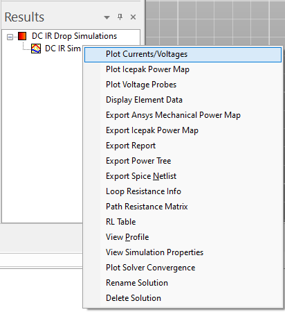
Complete these steps to view any of the following results.
- From the Results window, expand DC IR Drop Simulations.
- Right-click an appropriate simulation.
- Click a result type to open.
Plot Currents/Voltages
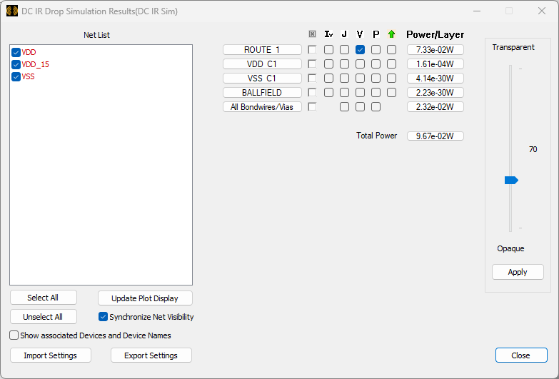
From the DC IR Drop Simulation Results window, select from the following combination of nets, layers, and element parameters to view plot overlays in the Modeling workspace:
- Net List area — check boxes to view nets with associated plots.
- Power Layer table — check boxes to view field quantities on any combination of layers. Only one type of field quantity (i.e., Iv (via current), J (current density), V (voltage), or P (power)) can be viewed at a time, but any combination of layers can be active. The Modeling workspace updates dynamically to show selected currents/voltages.
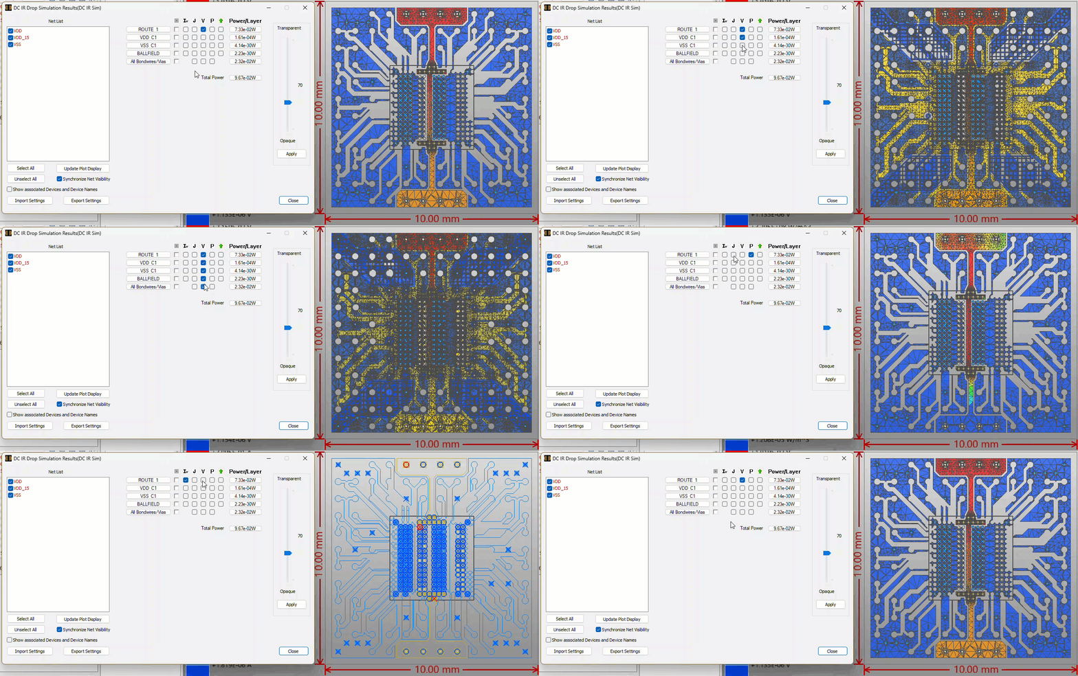
Check any box in the elevation column (i.e., the green arrow) to raise the component mesh in the Modeling workspace. Only available for components on metal layers.
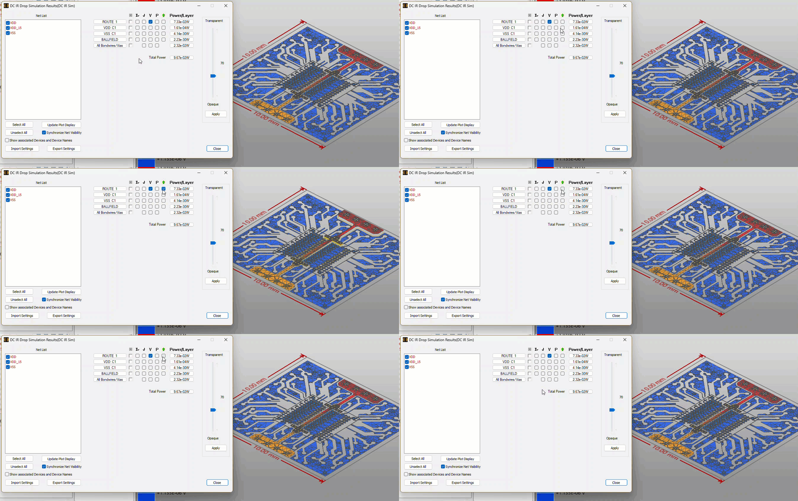
- Synchronize Net Visibility checkbox — check to return to default settings.
- Transparentslider — adjust the slider and click Apply to set element visibility.
- Import Settings — import previously saved settings as an XML file.
- Export Settings — save the current settings as an XML file.
Plot Icepak Power Map
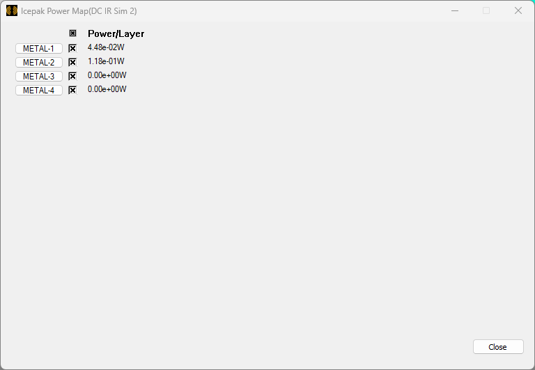
From the Icepak Power Map window, check boxes to select layers for which Icepak results display.
Plot Icepak Power Map only works if, during simulation setup, users check the Export power dissipation for use in Ansys Icepak and Mechanical box (i.e., located in the Compute DC Current and Voltage Distribution window > Ansys Icepak Options area. Refer to Computing DC IR Simulations.
Voltage Probe Plot
To immediately overlay a voltage probe plot in the Modeling workspace, click Plot Voltage Probes.
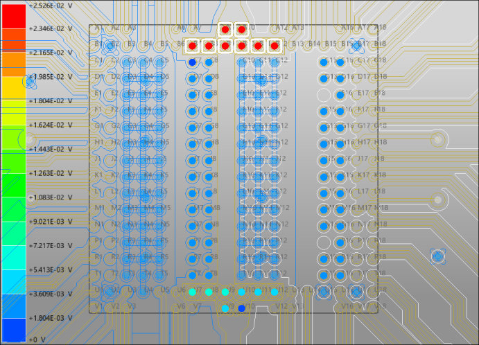
Right-click any voltage to highlight probes with that voltage (e.g., in the previous screenshot, the +2.526E-02 V probes are highlighted in white).
Display Element Data
From the DC Simulation Element Data window, select any combination of nets, layers, and element parameters to view plot overlays in the Modeling workspace:
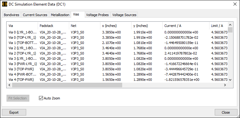
Selecting an element populates the Properties window with information about it. When Auto Zoom is enabled, selecting an element also zooms the Modeling workspace to that element. Elements are sorted into the following tabs:
- Bondwires — displays a list of bondwires. The Pass/Fail column displays Pass if the total current is less than or equal to the current limit flowing through the element (see: Technical Notes).
- Current Sources — displays a list of current sources, along with their voltage and current.
- Metallization — displays a list of areas with a specified voltage, current density, or power density. To populate the list, enter an appropriate information and click Find.
- Vias — displays a list of vias. The Pass/Fail column displays Pass if the total current is less than or equal to the current limit flowing through the element (see: Technical Notes).
- Voltage Probes — displays a list of voltage probes.
- Voltage Sources — displays a list of voltage sources.
Use the tabs to move between elements, and click column headers to sort the data. Click Export to save the data as a DC Element Data File (*.dc).
Loop Resistance Info
From the Loop Resistance window, make selections to see how the loop resistance is computed per pair of sources where the first source is the location of the measurement, and the second is the return path of the current loop. Note the source used as return path is shorted and the internal resistance is ignored.
Path Resistance Matrix
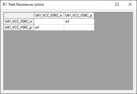
From the Path Resistances window, view the resistances between pairs of terminals.
RL Table
Select RL Table to open the DC RL Table window.
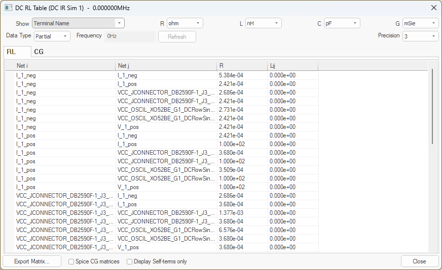
The RL table displays Q3D-like self and mutual resistance and inductance values computed by the DCIR solver in a list format. Every voltage and current source-based (i.e., driven) DCIR simulation includes a source with both a positive and a negative node, which are treated as terminals. During simulation, the solver selects one terminal on each net to designate as a sink, while the remaining n−1 terminals on that net are treated as sources. In DCIR terminal-based simulations, the terminal locations are set by the user, but the classification of source vs. sink follows the same logic as in driven simulations.
To measure resistance and inductance on a net, the solver injects 1 ampere (A) into each source terminal in turn and measures the voltage at all the source terminals, including the injection point, as the current flows to the designated single sink terminal.
Plot Solver Convergence
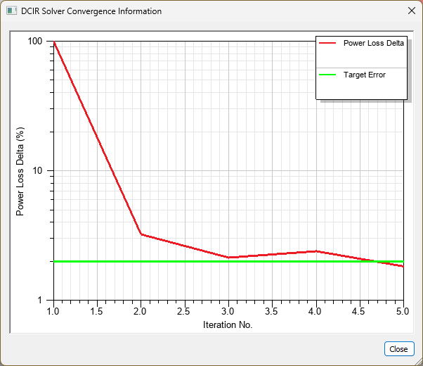
Select Plot Solver Convergence to open the DCIR Solver Convergence Information window.
