
Shell-to-Solid Contact Examples
The following guidelines involve contact between a shell object, or selected faces of a multifaced shell object, and coplanar or concentric faces of one or more adjacent solid objects. Three main variations are considered:
- A single shell in contact with a single solid object
- A single shell, which may represent an insulator or intermediate material, sandwiched between two solid objects
- A single shell object sandwiched between one large solid object and two or more smaller solid objects (used for the convenience of assigning contact at multiple interfaces with a single-object selection)
When a shell represents a thin object placed between two solids, such as the plastic or mica insulators often used to electrically isolate semiconductors from a heat sink, remember that there are actually three resistances to the flow of heat between the two solids:
- Contact resistance between the solid object on one side of the shell and the face of the shell
- The limited conductivity of the shell material through its thickness
- Contact resistance between the solid object on the opposite side of the shell and the face of the shell
Accounting for all three resistances requires that you correctly calculate the effective conductance or resistance value to specify in the assignment. See the examples that follow for more detail.
Additionally, a shell may be used only as a means of conveniently assigning contact between multiple small solid objects and a single larger solid object (such as many surface-mount components on a printed circuit board. In this case, you do not want to consider three resistances as described in the preceding insulator case. Since the software will effectively double the resistance you specify by assuming that it applies to the shell-to-solid interfaces on both sides of the shell, you must calculate the effective resistance to assign differently than for the insulator case. Again, see the examples that follow for more detail.
Examples and guidelines for various scenarios are as follows:
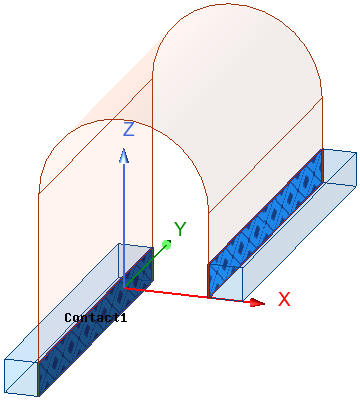
- Example 1: Contact between a single solid object and a single shell:
- Example 2: A shell is sandwiched between two solids, and you wish to treat it as an electrical insulator:
- The resistance or conductivity at a single solid-to-shell interface.
- The equivalent resistance or conductivity of the shell material for half of its thickness.
- Contact impedance per contact interface, Impedancecontact = 97 °C·mm2/W
- Material conductivity, k = 0.0006 W/(mm·°C)
- Insulator thickness, Thk = 0.076 mm
- Effective Impedance of shell material:
Impedancehalf-material = Thk/2 * 1/k = Thk / 2k
So, Impedancehalf-material = 0.076 mm / [2 * 0.0006 W/(mm·°C)] = 63.3 °C·mm2/W - Finally, the Impedance to assign = Impedancecontact + Impedancehalf-material = 97 + 63.3 = 160.3 °C·mm2/W
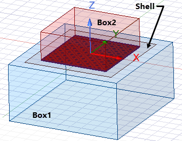
- Example 3: A shell object is sandwiched between one large solid object and multiple small solid objects. (In this case, the shell is used for the convenience of assigning solid-to-solid contact to multiple objects based on a single-shell selection):
- Contact conductance per area, Unit Conductance = 0.103 W/(°C·mm2)
- Effective contact conductance per area:
Unit ConductanceEff = Unit Conductance * 2 = 0.206 W/(°C·mm2) - The default shell object thickness is 1e-7 mm, which is less than a micron and is acceptable.
- Define a custom material with a thermal conductivity of 1e-6 W/(m·°C), which is orders of magnitude lower than the conductivity of air and therefore insignificant.
In this example, a single contact assignment is used for the face of each box that is in contact with the shell object. Since the actual contact area matches the total assignment face area, you can choose any Resistance Type. If you choose Thermal Conductance or Thermal Resistance, the specified value represents the total combined contact area of both selected faces (not the conductance or resistance per contact face).
You can assign contact to one of the solid object faces or to the shell object or face, which becomes the primary Contact face. The solver will find the other two adjacent solid or shell faces, and these will be the Target faces.
If you plan on specifying a total resistance or conductivity value, it is best to assign contact to the smallest of the three faces so that the contact area matches the selected face area. Otherwise, if you will used area-based options (Thermal Impedance or Thermal Conductance per Area), it doesn't matter which face you choose for the contact assignment.
The resistance you specify is doubled, or the conductivity is cut in half, because the solver will apply the resistance to contact interfaces on both sides of the shell. This behavior is consistent for all five Resistance Type options, including Thickness. That is, the thickness you specify is effectively doubled because the equivalent resistance calculated from the material conductivity and thickness is applied to contact interfaces on both sides of the shell.
When calculating the effective thermal contact resistance to specify in the contact definition, include the following two constituent values:
The solver will double the specified resistance, effectively accounting for two contact interfaces and the full thickness of the shell object.
Avoid using the Thickness option for the Contact Resistance Type unless you only want to consider the shell material's limited thermal conductivity and are assuming there is no contact resistance. An example of this usage is when the shell represents an epoxy film used to bond a component to a PCB or substrate, where the epoxy fills in surface roughness and provides a full contact area, mitigating thermal contact resistance. In this case, specify half of the actual epoxy film thickness, since the solver will double the equivalent resistance. Note that, if the shell is omitted, you can assign contact directly between the two solids, in which case you would use the full film thickness. Since there's no shell, there's a single contact interface, and the resistance is not doubled.
The following equations show how to calculate an effective Impedance value to assign to a solid-shell-solid sandwich so that the material's resistance and thermal contact resistance at both sides of the shell are included correctly:
Assume:
Therefore:
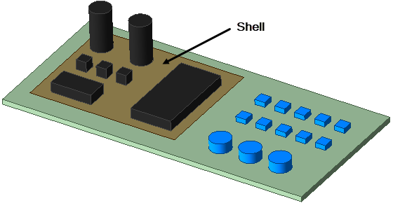
For this example, assume that the blue components on the right half of the model are bonded to the substrate without thermal resistance. The black components on the left half of the model are mounted to the substrate with a common thermal contact resistance assigned. Since approximately half of the substrate face has bonded contact, and the other half has areas of thermal contact resistance, contact cannot be assigned to this face. You could select all of the individual component bottom faces on the left half of the board for assigning contact. However, it might be more convenient to draw a shell object that encompasses all of the component-to-substrate interfaces to which you wish to assign contact. In this example, we use the latter approach, so the contact assignment includes only the shell object or its face.
For this application, we don't want to include the resistance of the shell material across its thickness. We also don't want the resistance to be doubled (representing contact interfaces on both sides of the shell). The solution is to specify either half of the contact resistance or double the contact conductivity in anticipation of the solver imposing the resistance twice.
Since the area of the shell face is much greater than the actual contact area, do not specify total Thermal Resistance or total Thermal Conductance. Instead, use an area-based contact resistance type (Thermal Conductance per Area or Thermal Impedance).
The following equations show how to calculate an effective Conductance per Area value to assign to a solid-shell-solid sandwich so that it correctly represents the thermal conductance that would occur between the components and substrate through a single contact interface (ignoring the shell):
Assume:
Therefore:
To prevent the shell from providing a redundant thermal conduction path along the surface of the substrate, specify an infinitesimal thickness in the shell object attributes and specify a material with negligible thermal conductivity.