
Assigning Layered Impedance Boundaries
A layered impedance boundary is used to model multiple thin layers in a structure as one impedance surface. The effect is the same as an impedance boundary condition, except that Ansys Electronics Desktop calculates the impedance of the surface based on data you enter for the layered structure, including surface roughness.
Materials with thermal modifiers can have layered impedance boundaries assigned to them. The layered impedance boundary is supported for single-frequency solutions and for Discrete and Interpolating frequency sweeps. The order of the layers does not matter to the implementation.
Layered impedance boundaries can be one sided or two sided. One-sided boundaries terminate their model in an infinite space, such as air or vacuum. Two-sided boundaries do not. Two-sided boundaries can be used in 3D models. By default, Ansys Electronics Desktop assumes the layered structure is one sided, external to the design.
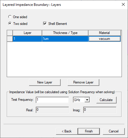
If the layered structure is within a 3D model, meshing thin layers and solving inside is inefficient. You can replace the highly conductive thin layer by a shell element. Shell elements are 3D layers that have been replaced by a sheet. They cannot represent a one-sided impedance boundary. The Shell Element option only applies to HFSS Driven solution types and does not apply to HFSS Eigenmode and Transient solution types or to HFSS-IE designs. Shell elements maintain two sets of unknown coefficients for the top and bottom surface. If the angle of incident deviates significantly from the boundary, then the accuracy of the shell elements degrades and you should use a layered impedance boundary instead.
Practical uses of shell elements in simulations include:
- an antenna inside a car chassis when the chassis is modeled using sheets
- an antenna inside a dielectric radome when the radome is modeled using sheets
If you specify that a two-sided sheet is to be modeled as a shell element, the following HSS features are disabled:
- Scattered field formulation: HFSS disables this when all boundaries are radiating boundaries AND when the design has an Incident Wave excitation.
- IE solver
To assign a layered impedance boundary:
- Select a surface
on which to assign the boundary and click HFSS> Boundaries>Assign>Layered Impedance
or HFSS>Boundaries>Assign>Surface Roughness> Groiss (Layered Impedance) ...to bring up the Layered Impedance
Boundary window.
- Click Next or the Layers tab, depending on the general option
setting.
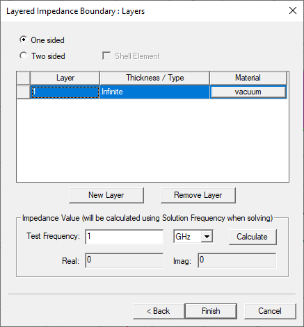
- If the layered structure is external to the design, do the following:
By default, Ansys Electronics Desktop assumes the layered structure is One sided, external to the design; the outermost layer of the structure is listed.
- Select whether this layer is an Infinite, Perfect E, or Perfect H layer from the Thickness/Type column.
- If the layered structure is within a 3D model, do the following:
- Select the Two sided option.
- Enter a thickness for the first layer in the Thickness/Type column. You can assign a variable as this value.
If it is a two-sided BC and not assigned to an SBR+ region, layer thickness should not exceed lambda/10 for for dielectric objects. For thin conductors, if the skin depth is much smaller than the layer thickness, you cannot replace it by an internal sheet.
Neither of these restrictions apply if the layered structure is part of an SBR+ region. For an SBR+ objects, there is no limit to the electrical thickness (i.e., measured in wavelengths) of the layers for result quality. However, it is not recommended that the absolute thickness of the layers exceed 20% of the lateral extent of the surface to which the BC is applied.
- To change the first layer's material, click vacuum and follow the procedure for assigning a material. The material properties that will apply to the layers can be functions of complex numbers.
- The Shell Element check box is for HFSS Driven situations where the layered structure is within the 3D model and you want to use sheets to model thin but finite thickness objects.
- To add a new layer to the structure:
- Click New Layer. The new layer is added at the end of the list.
- Enter a thickness for the layer in the Thickness/Type column. You can assign a variable as this value.
- To change the layer's material, click vacuum and follow the procedure for assigning a material.
- Optionally, to reorder layers, click the first row square and drag the row to the desired position.
- Optionally, to view the impedance values that will be calculated based on the data provided, do the following:
- Enter the frequency at which the solution is being solved in the Test Frequency text box.
- Click Calculate.
The real and imaginary components of the Ansys Electronics Desktop-calculated layered impedance value appear.
Enter the Surface Roughness for the layered structure.
If the layered structure is internal to the design, enter the average surface roughness of the two outermost sides. You can assign a variable as this value. Ansys Electronics Desktop uses the Groiss model for surface roughness. When surface roughness is activated, it is applied to the first conducting layer (not necessarily the first layer) for an external boundary, and to both the first and the last conducting layer for an internal boundary. - Click Finish to assign the boundary. The boundary appears under the Boundaries icon in the Project tree.

Optionally, you can use the Properties dialog to enter the Surface Roughness for a layered structure. Selecting the boundary displays the Properties.
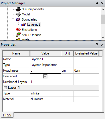
If the layered structure is internal to the design, enter the average surface roughness of the two outermost sides into the Roughness field. You can specify Units by clicking the drop-down menu in the Units column. You can assign a variable as this value. Ansys Electronics Desktop uses RMS deviation of the conductor surface from a plane. When surface roughness is activated, it is applied to the first conducting layer (not necessarily the first layer) for an external boundary, and to both the first and the last conducting layer for an internal boundary.
If a fast sweep is defined in a design that contains a layered impedance boundary, the impedance may only be accurate for the center frequency.