Viewing Circuit Elements
Your design can contain a number of circuit elements (capacitors, inductors, resistors, etc.). By default, all components are visible. You can choose to make all elements invisible, make all elements of a certain type invisible, or make an individual element invisible. Most of this is done in the Show/Hide area on the View tab.

Use the Show Mode drop-down menu to show all objects or only those currently selected.
Each icon on the right side of the Show/Hide area toggles the visibility of a certain element. Hover over the icons to see their associated actions. In order (from left to right, top to bottom), the icons are:
- View Non-Functional Pads
- View Antipads
- View Solderballs
- View Bondwires
- View Region Extents
- View Icepak Cabinet
- View 3D Regions
- View Capacitor Regions
- View Equipotential Regions
- Toggle Grid
- Toggle Grid Snap
- Display Mesh
- Display Surface Plot
- Display Color Scale
- Temperature Plots
- View Dielectric Layers
- View Dimension Marker
- View Coupled Structures
- View Pin Groups
Also on the View tab, the Labels section allows you to toggle visibility of labels and circuit element values.

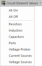
Use the Circuit Element Values drop-down menu to select the elements for which you would like to view values. Select All On to apply values to all circuit elements, and All Off to remove values from all circuit elements.

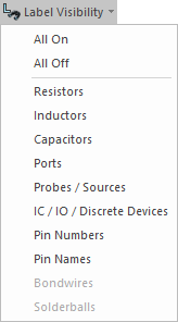
Use the Label Visibility drop-down menu to select the elements for which you would like to view labels. Select All On to apply labels to all circuit elements, and All Off to remove labels from all circuit elements.

