
Creating a Sample Pin Group, Step 2: Create a Component
Perform the following steps:
- Ctrl+click each pad to select all six pads.
- Click Advanced > Via.
- From the Pin Info area, specify the Type, Part Name and Reference Designator. The layer is already selected.
- Click OK.
The Via Properties window appears.

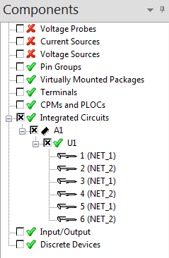
The component displays as a black box in the Modeling workspace, and appears in the Components workspace under Integrated Circuits.

To move the component to another category in the Components workspace, drag it under an appropriate category.