Editing Via Properties
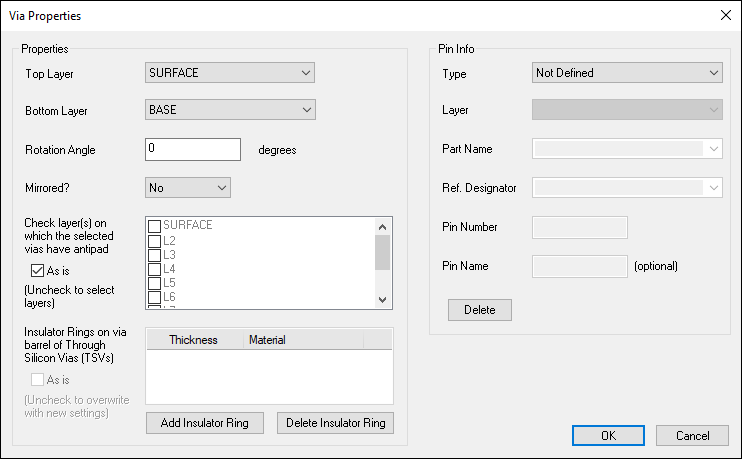
To edit via properties:
- Select one or more vias.
- Click Advanced > Via, or right-click a via in the Modeling workspace, and select Properties from the shortcut menu.
- Use the Top Layer and Bottom Layer drop-down menus to select the via layers.
- From the Rotation Angle field, type an angle in degrees to rotate the via in the XY plane. The rotation angle is specified from the orientation in the padstack and is counter-clockwise.
- Use the Mirrored? drop-down to specify whether the via layers are mirrored.
- From the Check layer(s) on which the selected vias have antipad, you can enforce antipad definition. By default, if a via is part of a net and crosses through a plane that it also part of that net, no antipad will be created regardless of the antipad definition in the padstack. This option forces selected layers to get an antipad, even if the via net is the same as the plane net that it is passing through. When multiple vias are selected, an As is option appears here, which leaves antipads as defined.
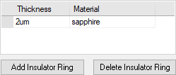
- Use the Add Insulator Ring and Delete Insulator Ring buttons as appropriate, or check As is to not change insulator rings. When an insulator ring is created, you can type the Thickness and select the Material of each ring. Only insulator materials are listed.
- From the Pin Info area, you can reassign pin names. Use the drop-down menus to select an appropriate pin and rename it using the Pin Name field. Click Delete to clear pin information.
- Click OK to accept the changes, or click Cancel to exit without making any changes.
The Via Properties window appears.

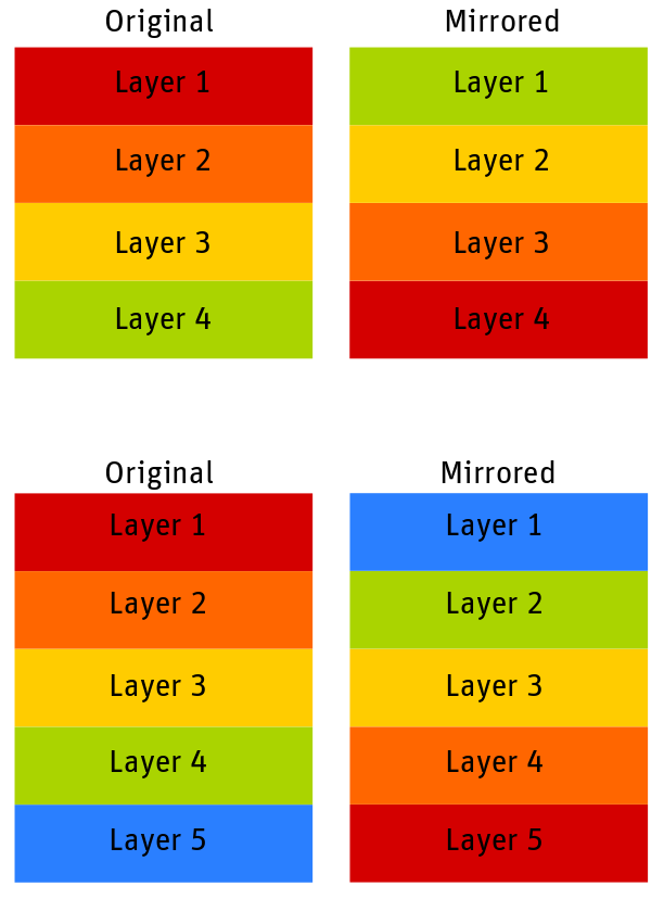
If your design has an even number of layers and you mirror those layers, the layers are mirrored in the following order: top layer is mirrored with the bottom layer and (top-n) layer is mirrored by the (bottom-n) layer
If you have an odd number of layers, the middle layer is mirrored around itself and the other layers are mirrored like even layers.
The graphic below shows the difference in mirroring for an even number of layers (top) and an odd number of layers (bottom).


TSVs (Through Silicon Vias) are vias that can pass through semi-conductor layers, such as silicon. They require insulator rings along the via barrel to prevent any electrical contact between the barrel and the semi-conductor layers through which they pass.
Simulation of TSVs is only supported in the PSI & CPA solvers within SIwave. If TSV rings exist on any via when another solver is run, a warning about TSV not being supported appears. You can acknowledge and proceed, or abort the simulation.
