
Assigning a Thin Layer Boundary for a 3D AC Conduction Solver
When two parts of the domain are separated by a thin volume, it can be modeled using a Thin Layer boundary condition. This boundary creates a field discontinuity (voltage drop) across the two sides of the surface based on the material bulk parameters and thickness.
This boundary condition can be used to model thin domains, for example: the contact resistance between two conductive domains, the capacitive effect of thin insulating materials or thin lossy domains in electronic boards without needing to explicitly model (and mesh) a 3D object having a finite thickness.
For the 3D AC conduction solver, the thin layer is defined by its bulk conductivity, permittivity, and thickness.
To define a resistive sheet boundary:
- Select the section of the geometry on which you want to apply the boundary condition (typically a sheet object or face of a 3D body).
- Click Maxwell 3D > Boundaries > Assign > Thin Layer to open the Thin Layer dialog box.
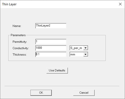
- Enter a name for the boundary in the Name box, or accept the default.
-
Enter the thin layer parameters in the Conductivity, Permittivity, and Thickness fields, and select the units of measure. Use of variables is supported.
-
Optionally, click Use Defaults to revert to the default values in the window.
The Defaults tab allows you to control default values. The Save Defaults button saves the values currently defined on the General tab as the defaults to be assigned to new boundaries. Revert to Standard Defaults clears existing user-defined values and replaces them with the standard default values.
- Click OK to assign the boundary to the selected object.
The Project Manager lists the newly assigned thin layer boundary in the tree. You can select the boundary in the tree to view and edit its properties in the Properties Window. You can also double-click the boundary entry in the tree to open it for editing in the thin layer dialog box.