
Printed Circuit Board (PCB)
PCB enables you to create geometry to represent an printed circuit board.
Use the navigation arrows on the image below to view each tab.
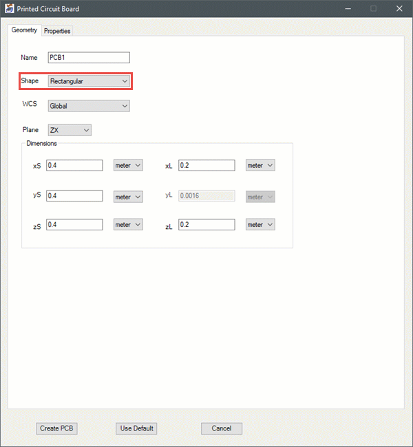
| Name | The Name appears in the Project Manager window, history tree, and 3D Modeler window. |
| Shape | Specify whether the PCB is rectangular or polygonal. |
| Plane | Specify on which plane the PCB lies. |
| WCS | Specify on which coordinate system the PCB is oriented. |
| Dimensions | For rectangular PCBs, define the start position relative to center and the length in the x, y, and z directions. For polygonal PCBs, specify the coordinates of the vertices (for example, vert 1, vert 2, vert 3, etc.) of the polygon. You can add and remove vertices using the Add and Rem buttons. |
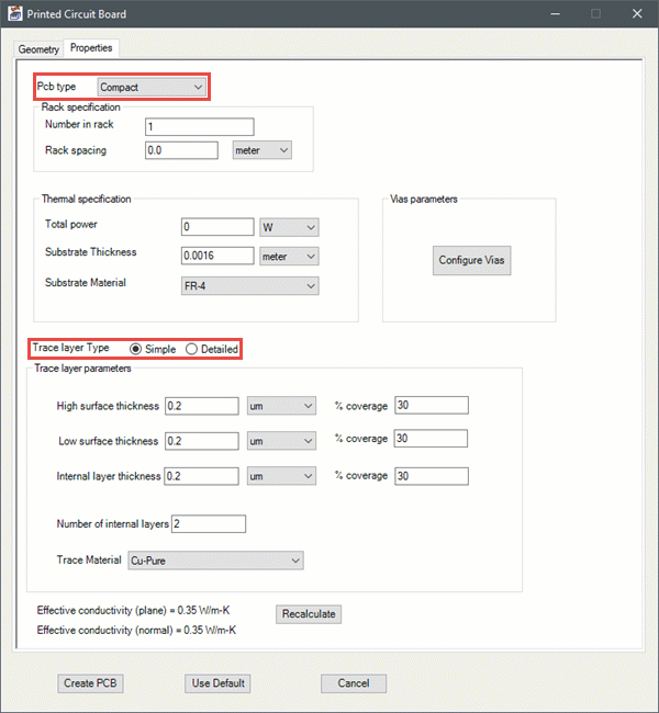
| PCB type | Specify whether the PCB is compact or detailed. |
| Rack specification | Specify the number of boards in the rack of PCBs. If you specify more than one board, you must also specify the Rack spacing between the boards. If you specify a positive value for the Rack spacing, the boards will be generated in the positive direction of the axis normal to the plane of the PCB. If you specify a negative value for the Rack spacing, the boards will be generated in the negative direction of the axis normal to the plane of the PCB. By default the spacing is set to zero. |
| Thermal specification | Specify a Total Power for the PCB. Also, specify the Substrate Thickness and then specify the Substrate Material to be used for the PCB. |
| Vias parameters | Click Configure Vias to display the Configure vias panel. Click Add to add as many vias as needed. Click Clear to remove all vias. Click Edit to edit a row. Click the delete button to delete a row. If you delete a row, the rows below it shift up and are re-numbered sequentially. |
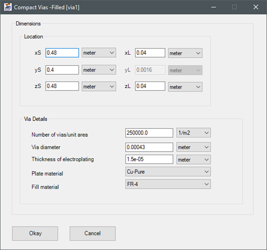
| Compact Vias-Filled dialog | Specify the Location of the vias. Enter the Via Details and click Okay. |
| Trace layer Type = Simple | |
|---|---|
| Trace layer parameters | For simple trace layers, specify the High surface thickness, Low surface thickness, and Internal layer thickness and then specify the % coverage for each under Trace layer parameters. Finally, specify the Number of internal layers and select the Trace Material. |
| Trace layer Type = Detailed | |
| Trace layer parameters | For detailed trace layers, you can create additional layers by clicking the Add layer button. Specify the Layer thickness, % coverage and Layer Material for each layer under Trace layer parameters. Click Delete layer to remove the last created layer. Finally, specify the Layer Material. |
| Recalculate | Click Recalculate to compute the effective conductivities (plane and normal). |
| Create PCB | Click Create PCB to insert the PCB in the Icepak design. |
| Use Default | Click Use Default to revert any changes you made to the default values. |
| Cancel | Click Cancel to close the dialog without creating a PCB. |
Iron Python Script – PCB.py:
The following is the toolkit's scripting information.
data = ["ng",
"Name:PCB",
'Length_unit:meter',
'Power_unit:W',
'via_area_unit:1/m2',
'Plane:ZX',
'Shape:Polygon',
'WCS:Global',
'Rectangle_dimensions:[0.4,0.4,0.4,0.2,0.0016,0.2]', #xs,ys,zs,xl,yl,zl
'Polygon_vertices:[[0.4,0.4,0.4],[0.6,0.4,0.4],[0.6,0.4,0.6],[0.4,0.4,0.6]]',
#x1,y1,z1
'Pcbtype:Compact',
'Numberinracks:3',
'Rackspacing:0.2',
'TotalPower:1',
'Substratethickness:0.0016',
'SubstrateMaterial:FR-4',
'TraceMaterial:Cu-Pure',
'Tracelayertype:Detailed',
'HighSurfacethickness:1e-6',
'LowSurfacethickness:1e-6',
'Internallayerthickness:1e-6',
'Numberofinternallayers:2',
'coverage_high:30',
'coverage_low:30',
'coverage_internal:30',
'Detailed_params:[[1e-6,30,"Cu-Pure"],[1e-6,30,"Cu-Pure"]]', #layer_thickness,
layer_coverage,layer_material
'via_params:[[0.48,0.4,0.48,0.04,0.0016,0.04, 250000,0.43e-3,15e-6,"Cu-Pure",
"FR-4"],[0.48,0.4,0.48,0.04,0.0016,0.04,250000,0.43e-3,15e-6,
"Cu-Pure","FR-4"]]' #xs,ys,zs,xl,yl,zl,vias_area,diameter,thickness,
Plate_material,Fill_material
]
oDesign.RunToolkit("SysLib", "Geometry/PCB_SCRIPT", [])
oDesign.RunToolkit("SysLib", "Geometry/PCB_SCRIPT", ['ng'])
oDesign.RunToolkit("SysLib", "Geometry/PCB_SCRIPT", data)