
Packages - PBGA
PBGA enables you to create geometry and boundary conditions to represent an plastic ball grid array package.
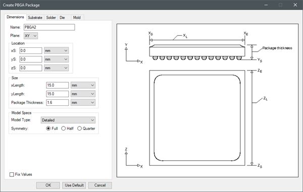
Use the navigation arrows on the image below to view each tab.
|
Name |
The Name appears in the Project Manager window, history tree, and 3D Modeler window. |
| Plane | Plane specifies the plane on which to create the package. |
| Location | Under Location, specify the starting coordinates for the package geometry relative to center of the 3D Modeler. |
| Size | Under Size, specify the length of the package in each coordinate direction. The coordinate direction represented by Package Thickness depends on the selected Plane. |
| Model Specs | Under Model Specs, specify the Model Type as Detailed, Compact Conduction Model (CCM), Characterize JC, or Characterize JB and select a Symmetry. |
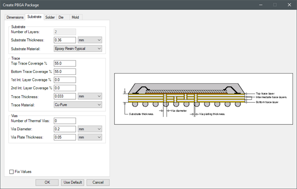
| Substrate | Under Substrate, specify the Number of Layers, Substrate Thickness, and Substrate Material. |
| Trace | Under Trace, specify the coverage percentage for the top trace, bottom trace, first internal layer, and second internal layer. Also specify the Trace Thickness and Trace Material. |
| Vias | Under Vias, specify the number of vias and via diameter and thickness. |
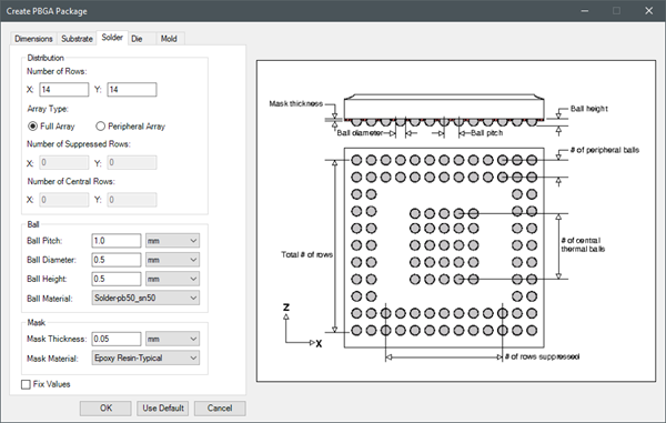
| Distribution | Under Distribution, enter the number of rows for solder balls, the Array Type. For a Peripheral Array, specify the number of rows to be suppressed and number of central rows. |
| Ball | Under Ball, specify the dimensions of the solder balls, including pitch, diameter, and height. Also, specify the material for the solder balls. |
| Mask | Under Mask, enter the solder ball mask thickness and material. |
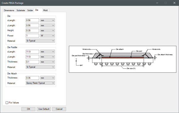
| Die | Under Die, specify the length of the die in each coordinate direction. The coordinate direction represented by Height depends on the selected Plane. Also, specify the die power and material. |
| Die Paddle | Under Die Paddle, specify the length of the die paddle in each coordinate direction. The coordinate direction represented by Thickness depends on the selected Plane. Also, specify the die paddle material. |
| Die Attach | Under Die Attach, specify the thickness of the die attach material and the material. |
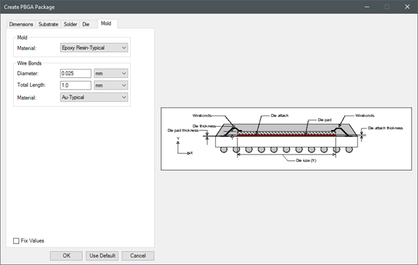
| Mold | Under Mold, select the material for the mold. |
| Wire Bonds | Under Wire Bonds, specify the diameter, average length, and material of the of the wire bonds. |
Iron Python Script – PBGA.py:
The following is the toolkit's scripting information.
data = ["ng",
'length_unit:meter',
'power_unit:W',
'Plane:XY',
'xS:0.0',
'yS:0.0',
'zS:0.0',
'Length1:0.015',
'Length2:0.015',
'Package Thickness:0.0016',
'Model Type:Detailed',
'Symmetry:Full',
'Substrate Thickness:0.00036',
'Substrate Material:Epoxy Resin-Typical',
'Top Trace:55.0',
'Bottom Trace:55.0',
'1st Int. Layer Coverage:0.0',
'2nd Int. Layer Coverage:0.0',
'Trace Thickness:0.000033',
'Trace Material:Cu-Pure',
'Number of Thermal Vias:0',
'Via Diameter:0.0002',
'Via Plate Thickness:0.00005',
'Number of Rows 1:14',
'Number of Rows 2:14',
'Array Type:Full Array',
'Suppressed Rows 1:0',
'Suppressed Rows 2:0',
'Central Rows 1:0',
'Central Rows 2:0',
'Ball Pitch:0.001',
'Ball Diameter:0.0005',
'Ball Height:0.0005',
'Ball Material:Solder-pb50_sn50',
'Mask Thickness:0.00005',
'Mask Material:Epoxy Resin-Typical',
'Die Length1:0.00856',
'Die Length2:0.00856',
'Die Height:.00035',
'Power:1',
'Die Material:Si-Typical',
'Pad Length1:0.0119',
'Pad Length2:0.0119',
'Pad Thickness:0.0001',
'Pad Material:Si-Typical',
'Attach Thickness:0.00036',
'Attach Material:Epoxy Resin-Typical',
'Mold Material:Epoxy Resin-Typical',
'Wire Diameter:0.000025',
'Wire Length:0.001',
'Wire Material:Au-Typical'
]
oDesign.RunToolkit("SysLib", "Geometry/Packages/PBGA", [])
oDesign.RunToolkit("SysLib", "Geometry/Packages/PBGA", ["ng"])
oDesign.RunToolkit("SysLib", "Geometry/Packages/PBGA", data)