
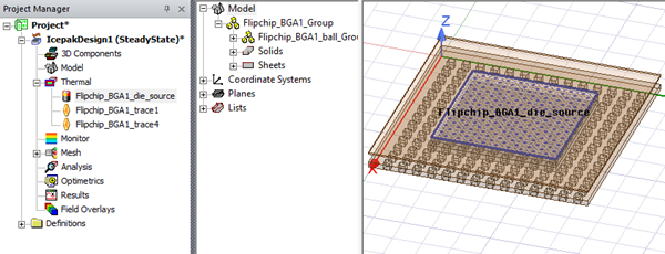
Packages - Flipchip_BGA
Flipchip_BGA enables you to create geometry and boundary conditions to represent a flipchip ball grid array package.
Use the navigation arrows on the image below to view each tab.
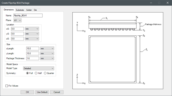
|
Name |
The Name appears in the Project Manager window, history tree, and 3D Modeler window. |
| Plane | Plane specifies the plane on which to create the package. |
| Location | Under Location, specify the starting coordinates for the package geometry relative to center of the 3D Modeler. |
| Size | Under Size, specify the length of the package in each coordinate direction. The coordinate direction represented by Package Thickness depends on the selected Plane. |
| Model Specs | Under Model Specs, specify the Model Type as Detailed, Compact Conduction Model (CCM), Characterize JC, or Characterize JB and select a Symmetry. |
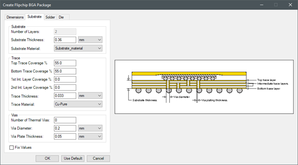
| Substrate | Under Substrate, specify the Number of Layers, Substrate Thickness, and Substrate Material. |
| Trace | Under Trace, specify the coverage percentage for the top trace, bottom trace, first internal layer, and second internal layer. Also specify the Trace Thickness and Trace Material. |
| Vias | Under Vias, specify the number of vias and via diameter and thickness. |
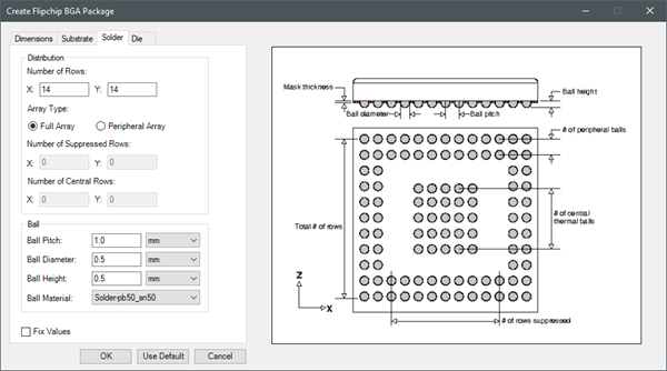
| Distribution | Under Distribution, enter the number of rows for solder balls, the Array Type. For a Peripheral Array, specify the number of rows to be suppressed and number of central rows. |
| Ball | Under Ball, specify the dimensions of the solder balls, including pitch, diameter, and height. Also, specify the material for the solder balls. |
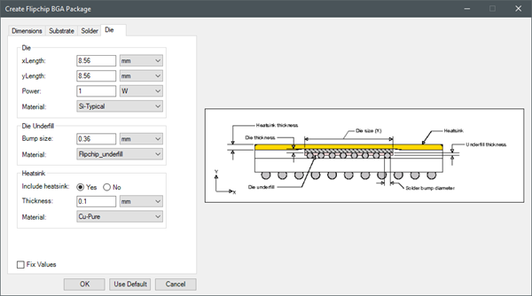
| Die | Under Die, specify the length of the die in each coordinate direction. Also, specify the die power and material. |
| Die Underfill | Under Die Attach, specify the bump size of the die underfill material and the material. |
| Heatsink | Under Heatsink, specify whether to include a heatsink in the package. If so, specify the heatsink thickness and material. |
Iron Python Script – Flipchip_BGA.py:
The following is the toolkit's scripting information.
data = ["ng",
'length_unit:meter',
'power_unit:W',
'Plane:XY',
'xS:0.0',
'yS:0.0',
'zS:0.0',
'Length1:0.015',
'Length2:0.015',
'Package Thickness:0.0016',
'Model Type:Detailed',
'Symmetry:Full',
'Substrate Thickness:0.00036',
'Substrate Material:Epoxy Resin-Typical',
'Top Trace:55.0',
'Bottom Trace:55.0',
'1st Int. Layer Coverage:0.0',
'2nd Int. Layer Coverage:0.0',
'Trace Thickness:0.000033',
'Trace Material:Cu-Pure',
'Number of Thermal Vias:0',
'Via Diameter:0.0002',
'Via Plate Thickness:0.00005',
'Number of Rows 1:14',
'Number of Rows 2:14',
'Array Type:Full Array',
'Suppressed Rows 1:0',
'Suppressed Rows 2:0',
'Central Rows 1:0',
'Central Rows 2:0',
'Ball Pitch:0.001',
'Ball Diameter:0.0005',
'Ball Height:0.0005',
'Ball Material:Solder-pb50_sn50',
'Die Length1:0.00856',
'Die Length2:0.00856',
'Power:1',
'Die Material:Si-Typical',
'Underfill Bump Size:0.00036',
'Underfill Material:Flipchip_underfill',
'Include Heatsink:Yes',
'Heatsink Thickness:0.0001',
'Heatsink Material:Cu-Pure'
]
oDesign.RunToolkit("SysLib", "Geometry/Packages/Flipchip_BGA", [])
oDesign.RunToolkit("SysLib", "Geometry/Packages/Flipchip_BGA", ["ng"])
oDesign.RunToolkit("SysLib", "Geometry/Packages/Flipchip_BGA", data)