
Traditional IBIS models supply tables of currents delivered to the output by the pullup, pulldown, power clamp and ground clamp structures. The current delivered at the output is the sum of those four contributions. With traditional IBIS models, the current drawn on the power rails is whatever the four structures draw to deliver to the output. Power Aware IBIS output buffer models contain additional information about the actual current drawn on the supply rails. They also contain information that allows the simulator to more accurately account for the effects of variations in the supply rail voltages.
Composite Current
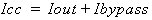
A [Composite Current] section in the IBIS file describes the shape of the rising or falling edge waveforms in the total current through the power reference terminal of the buffer. The composite current (Icc), the total current to be drawn through the power pin, is the sum of the current at the output (Iout) and the current internal to the device that goes to ground without reaching the output (Ibypass):
The IBIS file contains [Rising Waveform] and [Falling Waveform] tables of times and output voltages for the waveforms. The Electronics Desktop calculates the output current Iout based on the output voltage and the terminating load.
When the IBIS model file for an Output buffer contains a [Composite Current] section after a [Rising Waveform] or [Falling Waveform] table, Nexxim reads in the table of times and currents. The times in the composite current table are identical to the times in the corresponding waveform table. Nexxim calculates Ibypass at each time point by subtracting the output current on the composite current.
During simulation, Nexxim adds a current source to generate Ibypass between the power and ground pins of the power-aware Output buffer.
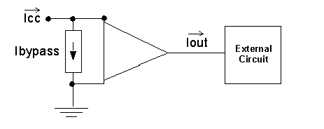
The current direction for Iout in the diagram has been reversed on the convention used in the IBIS specification, in order to simplify the formulas and discussion.
The current drawn on the power pin equals Icc, the current specified in the [Composite Current] table. The output current, Iout, is unchanged.
The composite current feature allows you to simulate with a non-ideal power supply and get accurate values for the power consumption. Power usage during events such as simultaneous switching operations (SSO) can be simulated accurately.
Gate Modulation Effect
The gate modulation effect is the change in output current Iout due to fluctuations in the gate voltage.
The [ISSO PU] and [ISSO PD] tables allow the simulation to account for variations in the gate current due to bouncing on the supply voltage.
Gate Modulation at the Pullup Node
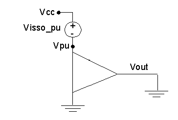
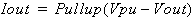
The [Pullup] section provides tables of output current Iout for values of the voltage drop (Vpu - Vout). Here is a reference diagram.
From the absence of gate modulation:
Vpu need not be equal to ideal voltage Vcc. Any voltage drop at the power pins affects the voltage difference between the power pin and the output pin, affects the lookup in the I-V table for the model.
The [ISSO PU] table gives the effective current of the pullup structure as a function of the voltage on the pullup reference node (the power node). When Nexxim finds an [ISSO PU] section after a [Pullup] entry, the calculation for Iout proceeds as follows.
- Nexxim calculates the voltage drop between Vpu and Vout and uses this value as before to look up Iout before the adjustment for gate modulation.
- Nexxim calculates the voltage difference between the ideal Vcc and the actual pullup voltage Vpu. This voltage difference is called Visso_pu in the diagram.
- Nexxim uses the value of Visso_pu to access the table in the [ISSO PU] section. The table gives the output current for that amount of voltage modulation, Iisso_pu.
- Nexxim accesses the [ISSO PU] table entry for Visso_pu=0V. The value of Iout at Visso_pu=0 is the nominal current, Inom_pu.
- Nexxim calculates a scale factor Kpu as the ratio of the tabulated output current to the nominal current:
- The final output current is the ideal output current on the [Pullup] table, scaled by the Kpu factor for the voltage modulation on the [ISSO PU] table:

Gate Modulation at the drop-down menu Node
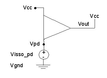
The [Pulldown] section provides tables of output current Iout for values of the voltage drop on the output voltage to the drop-down menu reference voltage (Vout - Vpd). Here is a reference diagram.
From the absence of gate modulation:

The [ISSO PD] table gives the effective current of the drop-down menu structure as a function of the voltage on the drop-down menu reference node (the ground node).
When Nexxim finds a [ISSO PD] section after a [Pulldown] entry, the calculation for Iout proceeds as follows.
- Nexxim calculates the voltage drop between Vout and Vpd and uses this value as before to look up Iout before the adjustment for gate modulation.
- Nexxim calculates the voltage difference between the actual pulldown voltage Vpd and the ideal ground reference Vgnd. This voltage difference is called Visso_pd in the diagram.
- Nexxim uses the value of Visso_pd to access the table in the [ISSO PD] section. The table gives the output current for that amount of voltage modulation, Iisso_pd.
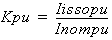
- Nexxim accesses the [ISSO PD] table entry for Visso_pd=0V. The value of Iout at Visso_pd=0 is the nominal current, Inom_pd.
- Nexxim calculates a scale factor Kpd as the ratio of the tabulated output current to the nominal current:
- The final output current is the ideal output current on the [Pulldown] table, scaled by the Kpd factor for the voltage modulation on the [ISSO PD] table:
