
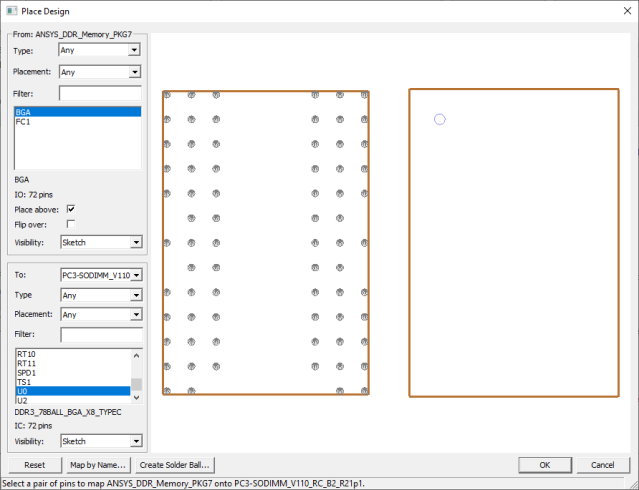
Place Design Window
The Place Design window configures how a subdesign is placed into an HFSS 3D Layout design. Click the Place Design window to capture or merge the relative positioning of one design to another.
To open the window, click a subdesign and a component the subdesign are connected to. From the menu bar, select Layout > Place Design. Also right-click the component and select Place Design. The window opens with one or two pairs of pins selected in the window.
Filters and Orientation
The subdesign From is what you are placing. The component To is what the subdesign is being connected to. Both panes contain controls that allow you to filter and orient components. You can leave all combo box filters left blank to see all components. The following controls are available:
- Type: Filter by component type (Any, IC, IO, Resistor, Capacitor)
- Placement: Filter by placement layer. The list shown is specific to its model. The filter includes “Any” plus all stackup layers in the model (e.g., Any, TOP, GND, R1+VCCFILL, R2+GNDFILL, VCC, BOTTOM).
- Filter: Field where users can filter components by name. Components with the specified Name, Type, and Placement Layer are displayed in the list box underneath the filter field.
- IO: Lists the number of pins in the selected component. The text changes based on the type of component selected (e.g., IO, IC, Resistor, Inductor, Capacitor, or Other.)
- Place above: Controls whether the subdesign is placed on and connects to the top layer of the "To" component. The control's default adjusts based on the selected components. This control is not available in the Footprint editor.
- Flip Over: When checked, this control flips the subdesign along the X axis , then rotates it to correctly map the pins of the "To" component. The control's default adjusts based on the selected components. This control is not available in the Footprint editor.
- Visibility: Determines how the components are rendered in the window.
HFSS 3D dynamic link subdesigns do not have components, so a Port Plane dropdown is showed instead of these component filter controls. A listbox is displayed showing the port instances in the selected port plane. The Port Plane dropdown can be used to filter port instances to a specific z plane (or "Any " can be selected to show all port instances). Port instances may be selected in the listbox or graphically selected in the previewer.
Preview
A preview of the subdesign placement is displayed. As pin pairs are selected, the preview is updated to show the new placement.
Mouse operations are supported similar to the main layout window:
- Shift+click and drag to move
- Ctrl+Shift+click and drag to zoom in/out
- Ctrl+click and drag to rotate
- Ctrl+click to rotate to predefined angles
A shortcut menu on the previewer provides additional controls.
The “From” subdesign can be dragged. When selected in plane, it can also be rotated with the handle that appears. Manual dragging/rotating is only used to assist pin pair selection in the previewer and doesn’t actually impact placement once the window is closed.
Reset reverts to the initial preview orientation/placement
Map By Name
Upon opening the Map by Name window with the corresponding button, the design is automatically placed by any matching pin pair names (using the full name, net name, and/or suffixes). Users can manually select pin names on the list boxes. The preview in the main window updates as pins are selected in the Map by Name window.
Create Solder Ball
Click Create Solder Ball to add and configure solder balls to the pins of the From component that connect to the To components.