
Simulating Circuits Containing N-Port Models from a Full-Wave Field Solver
This note looks at some of the issues involved in taking an N-port black box model from a full-wave field solver, such as HFSS or SIwave, and simulating it in a circuit tool, such as HSPICE, AEDT Circuit, or Nexxim. There are certain subtle differences between these models and the familiar low-frequency RLC equivalent circuit models from parasitic extractor tools like Q3D. In order to explain these differences, we will “open up” the N-port black box model and peek inside to see what is going on with its implementation. Armed with this information, we will then be able to better appreciate the capabilities and limitations of such models.
Some Background on Lumped Models
Consider a Spice subcircuit that consists of two resistors, R1 and R2, as shown below in Figure 1. The resistors in this case might represent the partial resistances for two nets, as computed by a tool like Q3D Extractor.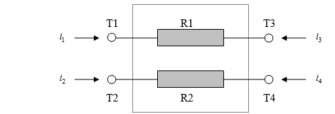
Figure 1: A conventional Spice subcircuit with two resistors.
This subcircuit has four terminals, labeled T1, T2, T3 and T4 in the figure. We can associate a node voltage with each of these terminals. We will call these  ,
,  ,
,  and
and  , respectively. It should be noted that these node voltages are measured with respect to some global ground reference—node 0 in Spice. We can also define a set of terminal currents, one for each terminal, called
  ,
,  ,
,  and
and  , respectively. For consistency, the direction of these terminal currents is taken to be “into” the subcircuit.
Given the structure of this subcircuit, we have a fair amount of flexibility. We could compute the resistance of the top net by hooking a current source across T1 and T3 and measuring the resulting voltage drop. We could do the same with the bottom net. Or we could measure the loop resistance by shorting T3 and T4 together, and putting a current source across T1 and T2 (and then measuring the resulting voltage drop between T1 and T2.)
You need to be very careful with how you use connections to ground in such a model. Consider the example shown below in Figure 2. On the top, we show an incorrect attempt at measuring the loop resistance. The problem is that the user has grounded both terminals, T2 and T4. This effectively shorts out the resistor R2, and so the apparent resistance will only be  . The correct way of setting up the circuit is to remove the ground at terminal T4; this allows us to measure the true loop resistance,
  .
.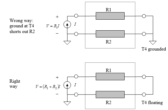
Figure 2: Illustration of the right (bottom) and wrong (top) ways to measure the loop resistance, in the case of a subcircuit consisting of standard RLC Spice elements.
As a general rule, when a conventional RLC circuit model is used, at most one terminal of the subcircuit should be connected to ground. If more than one terminal is grounded, you will be implicitly placing an ideal short circuit across those pairs of grounded terminals. The short circuit will bypass internal current flow paths, often resulting in unexpected behavior. Note that it is possible that none of the subcircuit’s terminals will be grounded; the connection to ground may be made through some external circuitry.
A 2-Port Model
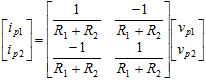
Now let’s consider creating a 2-port model of this same circuit. We could choose S, Y or Z parameters, or other more exotic descriptions, but these are all basically equivalent. For the purposes of this note, we will use Y-parameters.
The first step is to choose the ports. If we suppose that the two resistors represent a signal conductor and its ground return, then the logical place for the ports is between the two nets. We will set up the ports as shown Figure 3.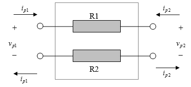
Figure 3: A 2-port model for the subcircuit.
Each port is created using a pair of terminals. Port 1 was created between terminals T1 and T2, and port 2 was created between terminals T3 and T4. We associate a port voltage ( and
and  ) and a port current (
 and
and  ) with each port. These port voltages and port currents are related to the terminal voltages and currents as follows:
|
|
 and and  |
(1) |
|
|
 and and  |
(2) |
|
|
 and and  |
(3) |
You will immediately notice that the ports have introduced some additional constraints that were not present before. In particular, due to the presence of the ports, the currents in the top and bottom resistors are no longer independent of one another. Whatever current enters the positive reference terminal (T1) for port 1 will flow back out of the negative reference terminal T2. Similarly, the current for port 2 goes into T3 and comes back out of T4. The placement of the ports in this circuit thus forces the bottom resistor to act as the return path for the current in the top resistor.
We now illustrate how the Y-parameters for this 2-port circuit are computed. Two voltage sources are connected at the ports, as shown in Figure 4 below. Illustration of how the Y-parameters for the 2-port circuit are computed. Two voltage sources are applied to control the port voltages, and the resulting port currents are calculated. These voltage sources directly control the port voltages and  .
.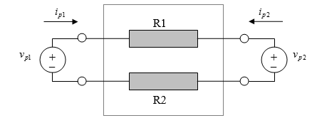
Figure 4: Illustration of how the Y-parameters for the 2-port circuit are computed. Two voltage sources are applied to control the port voltages, and the resulting port currents are calculated.
Using simple circuit analysis, the resulting port currents can be expressed in terms of the port voltages:
|
|
 |
(4) |
|
|
 |
(5) |
These relationships can also be expressed in matrix form as
|
|
 |
(6) |
The 2x2 matrix here is the admittance matrix (or Y-matrix) for the 2-port black box.
Observe that each of the Y-parameters depends on the sum  . Even if we measure all 4 matrix entries, we will never be able to determine the value of the individual resistances and
  from the Y-matrix. The information about the individual resistance values has been lost when we condensed the circuit down to a 2-port representation.
It is also interesting to compare the circuit of Figure 4 with the one in Figure 5 below. The Y-parameters of the two circuits will be found to be identical. Therefore, we have no way of distinguishing between the two networks if we have only their 2-port Y-parameter descriptions.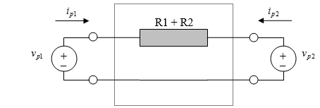
Figure 5. A different circuit that has the same Y-parameters as the one in Figure 4.
Implementing an N-port Network Model in a Circuit Simulator
An N-port network can be implemented within a circuit simulator by introducing N different 2-terminal circuit elements (or branches) as shown Figure 6. For each branch, the port voltage is taken to be the difference between the two node voltages at its terminals, and the port current is taken to be the current flowing in the branch. In addition to creating this element topology, the circuit simulator will be responsible for enforcing the branch relationships expressed in Equation 6 above.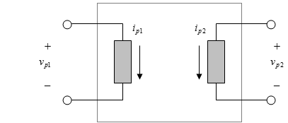
Figure 6. Illustration of how an N-port network is implemented within a circuit simulator, for the case of a 2-port network. In this topology, each port has its own reference node.
Another way of representing an N-port network is to use a common reference terminal, as shown in Figure 7 below. Because we will often choose to ground the negative reference terminal of a port, it may be more convenient to use this representation, because there are roughly half as many terminals to wire up. This is the approach taken by HSPICE (with the S element N-port S-parameter device) and also by Electronics Desktop (for imported S-parameter data.)
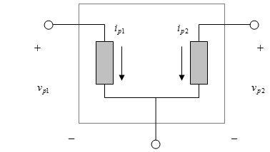
Figure 7. An N-port network with a common reference terminal (illustrated for the case of a 2-port).
Still another possibility is to suppress the reference terminal completely. In this case, the common reference terminal is internally wired to node 0. Only the positive reference terminals are exposed for external connections to the subcircuit. This is the approach taken by Electronics Desktop for dynamically linked field solver projects.
Using an N-Port Model for a Circuit Simulation
Let’s consider how we would use this circuit. Suppose that we want to evaluate the loop resistance for the two conductors. We will place a current source in parallel with port 1 and a short circuit across port 2 to create the desired current loop, and then we will measure the resulting voltage across port 1. The resulting circuit is shown in Figure 8. This experiment is essentially the same as the one that we conducted on the “conventional” Spice equivalent circuit illustrated in Figure 2 and so (at first glance) it seems reasonable to use the same circuit topology. However, now that we are working with the 2-port representation we will see some interesting differences in the details, although of course the final result will be the same.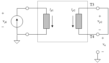
Figure 8. Computing the loop resistance using the 2-port black box model. This circuit looks correct (compare the bottom circuit of Figure 2) but actually causes simulation problems in Spice because the node voltage v4 at terminal T4 is ill-defined.
The first, and most important detail, is that the circuit simulator will probably fail if we try to simulate the 2-port circuit exactly as it is drawn in Figure 8. A typical error message would complain that there is “no DC path to ground” from the node corresponding to terminals T3 or T4. Another possibility would be an error message referring to a singular matrix, time step too small, Gmin stepping failed, or some other numerical problem.
What has gone wrong? The figure actually makes the problem fairly clear. Thanks to the short circuit, there is no question that the port voltage  is zero and hence the node voltages at terminals T3 and T4 are clearly the same. The problem is that these two node voltages are “floating” with no connection to ground, and so they could assume any values at all, as long as they are the same. An ill-defined problem of this sort is tantamount to a singular matrix equation—a system of equations with more unknowns than equations. Circuit simulators do not deal gracefully with this ambiguous situation, because they want to return specific values for the node voltages.
To make this a bit more rigorous, consider the problem of writing down the nodal Kirchhoff’s current law (KCL) equation at terminal T4. (This is what the circuit simulator will do internally.) We have a current leaving the node through terminal T3, and the same current  entering the node through terminal T4. As a result, the circuit simulator writes the equation
|
|
 |
(7) |
This, of course, is a tautology: 0 = 0. Because this equation effectively contributes no information about the circuit, the simulator is unable to come up with a unique solution.
The problem can be resolved by introducing some sort of DC conduction path between terminal T4 (or T3) and ground. One way would be to add a resistor between T4 and ground. The KCL equation at the node then becomes
|
|
 |
(8) |
Of course, all that this equation really says is that  . But that’s enough to give us a well-defined solution to the system of equations, and the circuit simulator will now succeed.
It’s interesting to note that the value of the grounded resistor we use is immaterial to the final solution. Because  no matter what value of resistor is used, we may as well simply connect terminal T4 to ground (node 0 in Spice.) The solution to the problem will not change.
Based upon previous experience with Spice, it may be tempting to use a large-valued resistor (perhaps in the giga-Ohm range) instead of a direct connection to ground. But Equation 8 shows that this is a bad idea. If we make the resistance too large, then  becomes vanishingly small and the equation again becomes equivalent (in the finite-precision arithmetic that computers use) to 0 = 0. In practice, what will happen is that the linear equation solver in the simulator will return increasingly inaccurate solutions as the value of the grounded resistor is increased. Therefore, using a large grounded resistor is a bad idea.
We should check what value of loop resistance will be returned by the simulator if we ground terminal T4. Looking back at Equation 4, we see that port voltage  , and therefore

and so we will have  . This is the correct value of the loop resistance.
In the case of the standard RLC Spice subcircuit, we argued that you should never connect more than one subcircuit terminal to ground. The reason for observing this practice was to avoid shorting out internal conduction paths in the internal RLC network. We have just seen that this same restriction does not apply to the 2-port model. We grounded two of the terminals, and yet we still obtained the correct loop resistance. How can this be?
Returning to the equivalent circuit model of a 2-port in Figure 6, we see that there are no internal circuit elements connected from the positive or negative terminals of port 1 to the positive or negative terminals of port 2. Therefore, it’s clear that we cannot accidentally short out an internal circuit element by grounding, unless we happen to ground both terminals of a single port.
There is one thing about the solution we obtained using the 2-port model that appears at first glance to be incorrect. If we refer back to the original Spice model (drawn at the bottom of Figure 2), it’s clear that the voltage at the “floating” terminal T4 is  , not zero. So is the 2-port model producing the wrong answer—or are we interpreting it incorrectly?
It turns out that the interpretation of the voltage is the problem. If we look back at the Y-matrix expression in Equation 6 , we see that it basically expresses port currents in terms of the port voltages. These port voltages are simply the voltage differences between the terminals, as expressed by Equation 1. We have previously argued (using Figure 5 as an illustration) that the N-port model has no way to tell whether the resistance lies in the upper or lower conductor. All it can do is to predict the correct voltage differences at the ports, given the port currents. So, because we have chosen to anchor terminal T4 to ground, the absolute voltage at this terminal disagrees with the predictions of the original subcircuit model. However, the voltage differences at the ports are in complete agreement.
We give a circuit interpretation of what is going on in Figure 9. Here we are taking the 2-port circuit of Figure 8 (with terminal T4 “grounded”) and re-drawing it with the real internal network of 2 resistors.
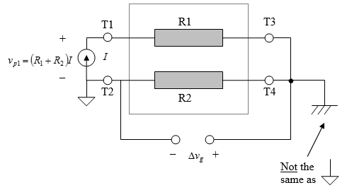
Figure 9. Interpretation of the different grounds being used in the two-port model.
 between the different grounds can easily be computed as