
Johanson 2450AT18D0100-EB1SMA
Abstract
This example is one of two Johanson Technology chip antenna and evaluation board (EVB) models that you can find in the Examples\HFSS\Antennas subfolder included in the Ansys Electromagnetics Suite installation. This model is associated with the following HFSS Getting Started guide:
Getting Started with HFSS: Matching Network – Using Tuning in Circuits
The example demonstrates the following:
- Using Johanson 3D Components
- Dynamically linking an HFSS design to a Circuit simulation
- Using lumped components and the tuning feature in the Circuit design to match the antenna (optimizing its performance)
- Generating several types of plots and overlays
- Pushing excitations from a Circuit design to an HFSS design

Figure 1: Johanson Chip Antenna and EVB with Overlaid 2D Gain Plots
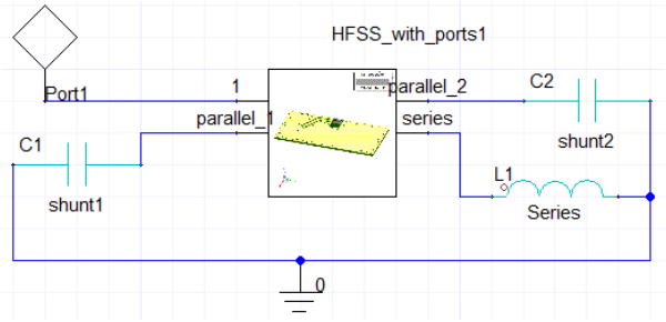
Figure 2: Matching Circuit Schematic
Version: 2024 R2
Simulation Time: 2 minutes: 20 seconds (using 8 cores), less than 1.4 GB RAM used
Model and Setup Details
The model consists of a single chip antenna mounted to an EVB – Johanson Technology, legacy part number: 250AT18D0100-EB1SMA. The antenna is a vendor model included as an encrypted 3D component. It is excited by a lumped port and contained within an automatically defined open region with a radiation boundary, as detailed below.
The example project contains three designs, summarized as follows:
- Circuit1: This design is dynamically linked to the third design (HFSS_with_ports). You can vary the discrete component values and immediately see the effect on the results. This is a fast and easy way of finding the ideal component values to optimize the design performance. You can then push the optimized parameters to the third design (HFSS_with_ports), where they are represented as lumped port excitations. For details on this process, refer to the Matching Network getting started guide referenced in the previous Abstract section.
- HFSS_with_lumped_RLC_imp (Modal Network): This design is the fastest and most straightforward way of determining the antenna and matching network performance when you do not intend to modify the RLC values. The tuning components are represented as lumped RLC boundaries. If you choose to modify any component value, you must run a new solution to see the updated behavior. Therefore, this method is not as desirable as the linked Circuit approach when the point of the analysis is to tune the component parameters for optimal results.
- HFSS_with_ports (Modal Network): In this design, tuning components are represented as lumped port excitations with renormalized impedances corresponding to the tuned component values pushed from the first design (Circuit1). When solved, this setup produces the same results as determined for the final tuned RLC component values in the Circuit design.
As an alternative approach to circuit tuning, you can substitute postprocessing variables for the renormalized impedance values. By varying the postprocessing variables, you can immediately see the effect of the design behavior (without having to rerun the solution). Similarly, you could scale the field amplitudes in the Edit Sources dialog box to see immediate tuning results.
This topic describes the setup of the HFSS antenna evaluation board solution and its results only. For details concerning the dynamic circuit link, adding lumped components for tuning, the tuning process, and pushing the excitations from the tuned circuit design to HFSS, see the above-referenced getting started guide.
The project filename and the design names differ between the example model and the getting started guide, but the setup procedure and results are otherwise the same.
Boundaries:
- Open Region with Radiation boundary (AutoOpen1), based on 2440 MHz adaptive solution frequency (HFSS > Model > Create Open Region)
- Finite Conductivity (FiniteCond1), 58 x 106 Siemens/m, classic infinite thickness model, at bottom face of PCB (HFSS > Boundaries > Assign > Finite Conductivity)
Excitations:
- Lumped Port (P1), 50 Ω impedance, single mode, at the beginning of the antenna feed
Mesh Setting:
- No mesh operations
- Initial Mesh Settings: Curved Surface Meshing slider three ticks coarser than default (to reduce the element count at the cylindrical grounding vias):

Figure 3: Initial Mesh Settings Dialog Box, Curved Surface Meshing Section
Setup:
- Bluetooth: 2440 MHz single solution frequency, Do Lamda Refinement enabled, 30% max refinement per pass, Auto Select Direct/Iterative selected, Save Fields enabled
- 1 – 4 GHz sweep in 0.001 GHz steps, 250 maximum solutions, 0.5% error tolerance
Postprocessing
After solving (Simulation > Analyze all), you can view different post-processing results. Look in the Project Manager under Results and double-click on the different predefined reports (Figure 4):

Figure 4: Predefined Reports Listed in the Project Manager
Predefined Reports:
Figures 5 through 10, which follow, show each of the six predefined reports in the HFSS designs of the example project. These results are based on the optimized matching network as solved in the third design (HFSS_with_ports). That is, the excitations have been pushed from the Circuit design to the linked HFSS design after tuning had been completed):

Figure 5: Smith Chart

Figure 6: S11 Plot (dB)

Figure 7: 3D System Gain Plot – Total Gain (dB) vs. Phi and Theta

Figure 8: Gain Plot 2 – Total Gain (dB) vs. Theta, Phi = 0°

Figure 9: Gain Plot 3 – Total Gain (dB) vs. Theta, Phi = 90°

Figure 10: Gain Plot 4 – Total Gain (dB) vs. Phi, Theta = 90°
Overlaying Reports on the Model Geometry:
To overlay any of the gain plots on the model geometry, right-click in the Modeler window and choose Plot Fields > Radiation Field from the shortcut menu. In the Overlay Radiation Field dialog box that appears, select the checkbox in the Visible column for one or more of the available gain plots and click Apply. Adjust the Transparency or Scale as desired and click Apply again. Click Close when finished. Figure 11 below shows the first (3D) gain plot overlay:

Figure 11: 3D System Gain Plot Overlaid on the Model Geometry