Co-Planar Waveguide (Driven Terminal)
The coplanar waveguide CPW consists of a signal trace sandwiched between two coplanar ground conductors. The width of the signal trace and the gap between the trace and the ground conductors affect the characteristic impedance. Model a short length as shown below and to obtain a longer length of the model you can deembed out of the port.
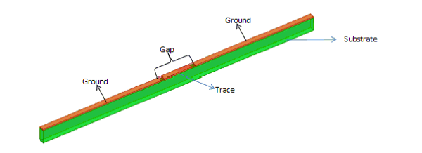
Figure 1 CPW (air box + ports hidden)
Define the ports such that only their faces touch the air box. The edges of the ports should not touch the edges of the air box.
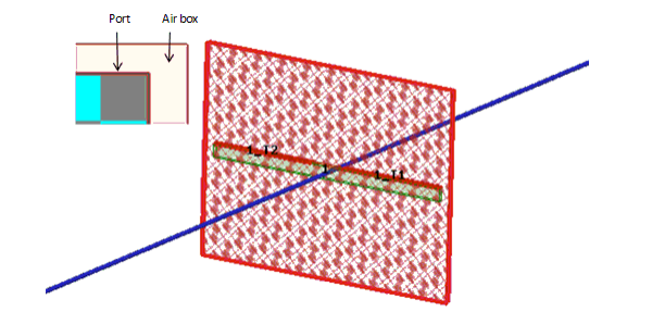
Figure 2 ports with dembeddding
Define the Radiation boundary only along the thickness of the air box. Assigning a radiation boundary on all surfaces of the air box in this model can make the port boundary to be conducting.
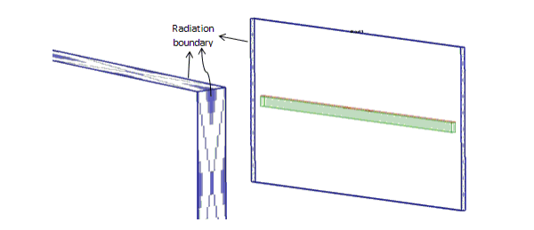
Figure 3 Radiation Boundary
Define a perfect H boundary on the air box. The wave port touches a perfect H boundary and therefore becomes an open circuit.
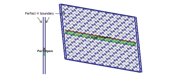
Figure 4 Perfect H boundary
So, the port boundary does not stay as a conductor anymore and almost mimics a “perfect open.” This is because with the application of the perfect H boundary “behind” the wave port, the port boundary becomes an open and will no longer be one of the conductors associated with the port. Now with three conductors namely, the two grounds and the trace, there are two possible modes that this structure can carry. Obviously, for the CPW structure we are interested in the center conductor excited at a voltage with reference to the two sides (or what we arbitrarily call “ground”) conductors at zero potential. Since voltage values can be arbitrary, this same mode could also be considered as the center conductor at “0” volt with the two side conductors at some equal voltage offset from the center conductor. In the terminal framework such a mode can be described as the center conductor labeled “reference” conductor with the two outside conductors considered to be the “terminals.” Then, by placing those two conductors at equal potential with respect to the center conductor they can be defined as differential pair whose common mode is the aforementioned mode of interest.
The Edit Post Process Sources dialog is shown below.
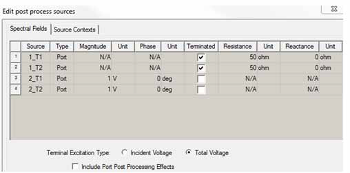
Figure 5 Edit Port Process Dialog
Notice from the plots below how the field gets trapped in the signal trace and dielectric.
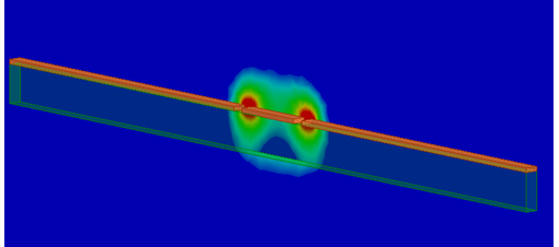
Figure 6 E field Plot
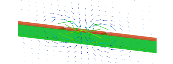
Figure 7: Vector Field
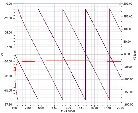
Figure 8 S-Parameter plot for the differential pair (legend shown below)