
|
Library: Basic Elements |
Modeling Language: SML |
Version Number: Twin Builder 2024.2 |
![]()
Figure 1. Component symbol
The BJT model is a modular model with definable simulation levels. Different simulation depths can be selected for the electrical and thermal behavior of the model.
You can define two simulation levels for the electrical and three simulation levels for the thermal behavior. Each level combination has a certain set of parameters. The values of them can be defined in the model dialog box. The component outputs are true of all types of the BJT models. They are listed at the end of the model description.
See also Dynamic Diode Model.
Electrical Model
The model uses an electrical equivalent circuit as shown in the following figure.
|
|
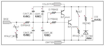
Figure 2. Equivalent circuit used for the Dynamic BJT model
There are two simulation levels regarding the electrical behavior. The level is set at the parameter TYPE_DYN:
TYPE_DYN=0
Only the static behavior is calculated. The charges at the capacitances are ignored, no switching behavior.
TYPE_DYN=1
In addition to the static behavior, charging and discharging of the junction and diffusion capacitances are calculated.
Electrical Behavior Level, Type DYN=0
The two BJT models for normal and inverse operation determine the static transistor current. In the normal operation mode, where the internal base-emitter voltage and the collector-emitter voltage are above 0 V, the current gain values for the BJT models are calculated from:
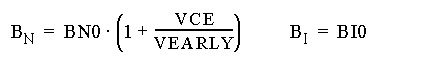
In the inverse mode:
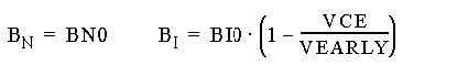
The static collector current is calculated from the base currents of the BJT models, and the base currents of the BJT models are calculated from their base-emitter voltages as following:
where VBE is the base-emitter voltage of the FET, and M is the ideality factor. The temperature voltage VT is calculated as following:
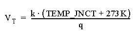
where k is the Boltzmann constant, and k=1.381E-23; q is the elementary charge, and q=1.602E-19.
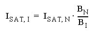
The saturation voltage of the BJT model for normal mode is calculated as following:
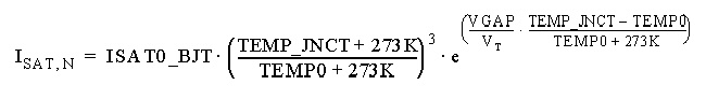
The saturation voltage of the BJT model for inverse operation is calculated as following:
The model has built-in fault detection. During the simulation the collector current and the base current, the voltage drops across base-emitter and collector-emitter as well as the junction temperature is observed. If their limitations are exceeded the model behavior changes. The switches controlled by the FAULT flags are closed and the respective fault resistances determine the model characteristic. Faults at the base do only affect RFAULT_BE. All other faults affect the RFAULT_CE.
Electrical Behavior Level, Type DYN=1
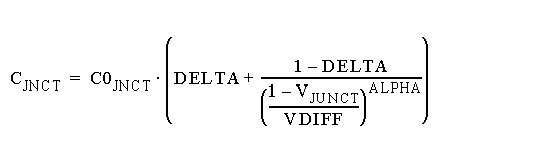
Junction capacitance:
There is a distinction between the calculation of depletion and enhancement capacitance behavior. The curves remain differentiable even at the transition from one region to the other. The transition happens if the junction voltage is less than 0 V.
If the junction voltage is greater than 0 V, the following equation is used:
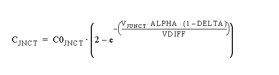
If the junction capacitance is negative (depletion region), the following equation is used:
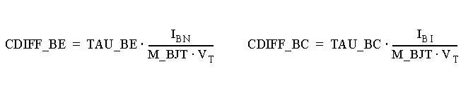
Diffusion capacitances (base-emitter, base-collector) can be calculated as following:
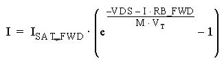
FWD Model
The FWD model is a static one only. The static current follows the formula:
Netlist generated by Special Component Dialog.
Select the netlist of interest below.
• NPN6
• NPN_FWD6
• PNP6
• PNP_FWD6
Table 1
| Name |
Port/Terminal Description |
Nature/Data Type |
| BASE |
Base |
electrical |
| EMITTER |
Emitter |
electrical |
| COLLECTOR |
Collector |
electrical |
Table 2. Parameters of TYPE DYN=0
| Name |
Description [Unit] |
Data Type |
| BN0 |
Normal Current Gain |
real |
| ALPHA_BN |
Exponential Temperature Coefficient of BN |
real |
| BI0 |
Inverse Current Gain |
real |
| ALPHA_BI |
Exponential Temperature Coefficient of BI |
real |
| VEARLY |
Early Voltage [V] |
real |
| ALPHA_VEARLY |
Exponential Temperature Coefficient of VEARLY |
real |
| M0 |
Ideality Factor of Base Junction |
real |
| ALPHA_M |
Exponential Temperature Coefficient of Base Junction Ideality Factor |
real |
| ISAT0 |
Saturation Current of Base Junction [A] |
real |
| ALPHA_ISAT |
Exponential Temperature Coefficient of Base Junction Saturation Current [A] |
real |
| RB0 |
Bulk Resistance of Base Junction [Ohm] |
real |
| ALPHA_RB |
Exponential Temperature Coefficient of Base Junction Bulk Resistance |
real |
| VGAP |
Band Gap Voltage [V] |
real |
| RC |
Collector Connector Resistance [Ohm] |
real |
| RB |
Base Connector Resistance [Ohm] |
real |
| RE |
Emitter Connector Resistance [Ohm] |
real |
| TEMP0 |
Reference Temperature [oC] |
real |
| VBREAK_CE |
Breakthrough Collector-Emitter Voltage [V] |
real |
| VBREAK_BE |
Breakthrough Base-Emitter Voltage [V] |
real |
| IBREAK_C |
Breakthrough Collector Current [A] |
real |
| IBREAK_B |
Breakthrough Base Current [A] |
real |
| TEMPBREAK |
Breakthrough Junction Temperature [oC] |
real |
| RFAULT_CE |
Collector-Emitter Resistance after Fault |
real |
| RFAULT_BE |
Base-Emitter Resistance after Fault [Ohm] |
real |
Table 3. Parameters of TYPE DYN=1 (+ Parameters of TYPE DYN=0)
| Name |
Description [Unit] |
Data Type |
| VNOM |
Nominal Voltage [V] |
real |
| INOM |
Nominal Current [A] |
real |
| C0_BE |
Base-Emitter Reference Capacitance [F] |
real |
| VDIFF_BE |
Diffusion Potential of Base-Emitter Capacitance [V] |
real |
| ALPHA_BE |
Capacitance Exponent Base-Emitter |
real |
| DELTA_BE |
Influence of constant capacitance at Base-Emitter |
real |
| ALPHA_CBE |
Exponential Temperature Coefficient of Base-Emitter Depletion Capacitance |
real |
| C0_BC |
Base-Collector Reference Capacitance [F] |
real |
| VDIFF_BC |
Diffusion Potential of Base-Collector Capacitance [V] |
real |
| ALPHA_BC |
Capacitance Exponent Base-Collector |
real |
| DELTA_BC |
Influence of constant capacitance at Base-Collector |
real |
| C0_CE |
Collector-Emitter Reference Capacitance [F] |
real |
| VDIFF_CE |
Diffusion Potential of Collector-Emitter Capacitance [V] |
real |
| ALPHA_CE |
Capacitance Exponent Collector-Emitter |
real |
| DELTA_CE |
Influence of constant capacitance at Collector-Emitter |
real |
| TAU_BE |
Carrier Lifetime at Base-Emitter Junction [s] |
real |
| ALPHA_TAU_BE |
Temperature Coefficient of Base-Emitter Carrier Lifetime |
real |
| TAU_BC |
Carrier Lifetime at Base-Collector Junction [s] |
real |
| ALPHA_TAU_BC |
Temperature Coefficient of Base-Collector Carrier Lifetime |
real |
| LC |
Collector Connector Inductance [H] |
real |
| LB |
Base Connector Inductance [H] |
real |
| LE |
Emitter Connector Inductance [H] |
real |
Table 4. Parameters of FWD Model
| Name |
Description [Unit] |
Data Type |
| M_FWD |
Ideality Factor of FWD |
real |
| ISAT0_FWD |
Saturation Current of FWD at TEMP0 [A] |
real |
| RB_FWD |
Bulk Resistance of FWD [] |
real |
Input/Output Quantities
Table 5
| Name |
Description [Unit] |
Data Type |
| VBE |
Base-Emitter Voltage [V] |
real |
| VBC |
Base-Collector Voltage [V] |
real |
| VCE |
Collector-Emitter-Voltage [V] |
real |
| IC |
Current through Collector Connector [A] |
real |
| IB |
Current through Base Connector [A] |
real |
| I_B |
Current through Base of Internal Static Model [A] |
real |
| CBE |
Base-Emitter Capacitance [F] |
real |
| CBC |
Base-Collector Capacitance [F] |
real |
| CCE |
Collector-Emitter Capacitance [F] |
real |
| TEMPJNCT |
Junction Temperature [oC] |
real |
| TEMPINTR |
Chip Temperature [oC] |
real |
| TEMPC |
Case Temperature [oC] |
real |
| PEL |
Total Component Losses [W] |
real |
| PCOND |
Power Transfer by Conduction [W] |
real |
| PCONV |
Power Transfer by Convection [W] |
real |
| PRAD |
Power Transfer by Radiation [W] |
real |
| ESWITCH |
Losses of One Switching Cycle [Ws] |
real |
| PSWITCH |
Average Losses of One Switching Cycle [W] |
real |
| ETOT |
Total Losses During Simulation [Ws] |
real |
| PTOT |
Total Average Losses During Simulation [W] |
real |
| FAULT_VCE |
Flag Collector-Emitter Over voltage |
real |
| FAULT_VBE |
Flag Base-Emitter Over voltage |
real |
| FAULT_IC |
Flag Collector Over current |
real |
| FAULT_IB |
Flag Base Over current |
real |
| FAULT_TEMP |
Flag Over temperature |
real |
This example demonstrates the operation mechanism of the advanced dynamic NPN BJT model through a simple example. The control base current is supplied by a pulse-wave voltage source E2. The schematic of the example is shown in Figure 3, system parameters are listed in Table 6, and the turn-on transient waveforms of the BJT model are shown in Figure 4.
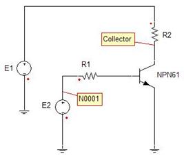
Figure 3. Application example of the NPN BJT model (advanced dynamic)
Table 6. System Parameters
| Component |
Parameter |
Value [unit] |
| Resistor R1 |
R |
10 [Ohm] |
| Resistor R2 |
R |
50 [Ohm] |
| Voltage Source (Pulse) E2 |
AMPL |
5 [V] |
| FREQ |
5000 [Hz] |
|
| TDELAY |
0 [s] |
|
| PHASE |
0 [degree] |
|
| OFF |
0 [V] |
|
| Voltage Source E1 |
EMF |
50 [V] |
* All the parameters of the NPN BJT model NPN61 use their default values, therefore they are not included in the parameter table.
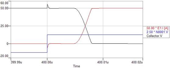
Figure 4. Simulation results-turn-on transients of NPN61
[1] Ned Mohan, Tore M. Undeland, William P. Robbins, "Power Electronics: Converters, Applications, and Design." John Wiley & Sons, INC. New York, 1995.