To specify a BGA package, select PBGA, Cavity Down BGA, FPBGA, or Flip-Chip from the Package type drop-down list in the Dimensions tab of the Packages panel (Figure 25.5: The Packages Panel (Dimensions Tab)).
The steps for defining a BGA package are as follows:
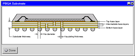
Specify the substrate parameters in the Substrate tab (Figure 25.6: The Packages Panel (Substrate Tab)).
Specify the Substrate thickness.
Specify the Substrate material to be used for the package. To change the substrate material for the package, select a material from the Substrate material drop-down list. See Material Properties for details on material properties.
Specify the Number of thermal vias in the substrate.
Specify the Via diameter and the Via plate thickness.
Specify the Top trace coverage %. This value is the percentage of the top trace layer volume represented by the copper coverage.
Specify the Bottom trace coverage %. This value is the percentage of the bottom trace layer volume represented by the copper coverage.
Specify the 1st int. layer coverage %. This value is the percentage of the first intermediate layer volume represented by the copper coverage.
Specify the 2nd int. layer coverage %. This value is the percentage of the second intermediate layer volume represented by the copper coverage.
Specify the Trace material. You can change the trace material by selecting a material from the Trace material drop-down list. See Material Properties for details on material properties.
Specify the Trace thickness. This is the thickness of each trace layer in the substrate.
You can modify the values of an imported trace by clicking the Edit traces button (only available after importing a anf, BOOL+INFO, ODB++, or IPC2581 file). You can change the values in the Board layer and via information panel. See Importing Trace Files for details.
(Optional) Click the Schematic button to open the Package Substrate panel (for example, Figure 25.11: The PBGA Substrate Panel) and view a schematic drawing of the package substrate.
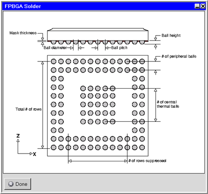
Specify the solder parameters in the Solder tab (Figure 25.7: The Packages Panel (Solder Tab)).
Specify the number of rows and columns of solder balls by entering values in the fields.
Specify the Array type. There are two options:
Full specifies that the ball grid will encompass the entire underside of the package.
Peripheral specifies that the main ball grid will encompass only the periphery of the underside of the package.
(peripheral arrays only) Specify the number of rows and columns of solder balls that are to be removed from the center of the grid by entering values in the fields next to # of rows suppressed.
(peripheral arrays only) Specify whether to include Central thermal balls in the array by selecting Yes or No.
If you select Yes, specify the number of rows and columns of balls that are to be added to the center of the array by entering values in the fields next to # of central rows.
Note: This option is not available for cavity-down BGA packages.
Specify the Pitch.
Specify the Ball diameter and Ball height.
Specify the Ball material. To change the Ball material for the package, select a material from the Ball material drop-down list. See Material Properties for details on material properties.
Select Block or Cylinder to represent the solder balls or solder bumps.
Note: Cylindrical geometry will imply larger mesh counts and increased computational costs.
(PBGA and FPBGA packages only) Specify the Mask thickness. This is the thickness of the solder mask.
(PBGA and FPBGA packages only) Specify the Mask material. You can change the mask material by selecting a material from the Mask material drop-down list.
(Optional) Click the Schematic button to open the Package Solder panel (for example, Figure 25.12: The FPBGA Solder Panel) and view a schematic drawing of the package solder.
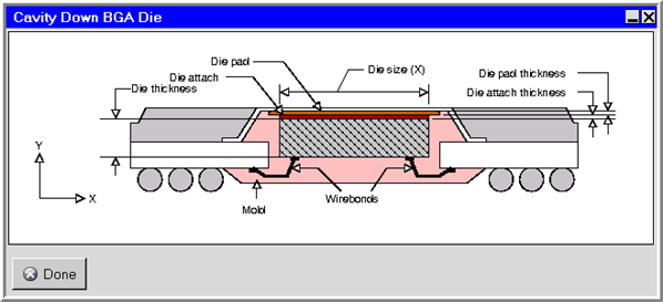
Specify the die and mold parameters in the Die/Mold tab (Figure 25.8: The Packages Panel (Die/Mold Tab)).
Specify properties for the Die.
If there is more than one die, you can select the appropriate die from the Current die drop-down list.
In the Die settings tab, specify the die Material. You can change the die material by selecting a material from the Material drop-down list. See Material Properties for details on material properties.
Specify the die Size and Thickness. To specify the size, enter values for the length and width of the die in the two fields next to Size.
Specify the Total power source that is distributed on the die surface. For half and quarter symmetry, you should still input the full power. There are two options to describe total power:
Constant enables you to specify a constant value for the Total power. This option is default for steady state problems and Compact Conduction Model (CCM) model types.
Temp dependent enables you to specify power as a function of temperature. Click the Edit button to display the Temperature dependent power panel. Inputs for the Temperature dependent power panel are described in Solid and Fluid Blocks.
Note: Transient problems are not supported for the Temp dependent option.
(For cavity-down BGA packages only) Specify the Cavity depth.
(For flip-chip packages only) Specify properties for the Die underfill.
Specify the die underfill Material. You can change the die underfill material by selecting a material from the Material drop-down list. See Material Properties for details on material properties.
Specify the die underfill Thickness.
(For PBGA or FPBGA packages only) Specify effective properties for the Die pad.
Specify the die pad Material. You can change the die pad material by selecting a material from the Material drop-down list. See Material Properties for details on material properties.
Specify the die pad Size and Thickness. To specify the size, enter values for the length and width of the die in the two fields next to Size.
(For PBGA, cavity-down BGA, and FPBGA packages only) Specify properties for the Die attach.
Specify the die attach Material. You can change the die attach material by selecting a material from the Material drop-down list. See Material Properties for details on material properties.
Specify the die attach Thickness.
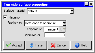
Specify the Top side radiation properties for the package.
If you select Top side radiation and then click Edit, Ansys Icepak will open the Top side surface properties panel (Figure 25.13: The Top side surface properties Panel).
Specify the Surface material to be used for the top side of the package. By default, this is specified as default. This means that the material specified for the side of the package is defined in the Basic parameters panel (see Default Fluid, Solid, and Surface Materials). To change the material for the top side of the package, select a material from the Material drop-down list. See Material Properties for details on material properties.
If the top side of the package is subject to radiative heat transfer, select Radiation. You can modify the default radiation characteristics of the package (for example, the view factor). See Radiation Modeling for details on radiation modeling.
(Optional) Click the Schematic button to open the Package Die panel (for example, Figure 25.14: The Cavity Down BGA Die Panel) and view a schematic drawing of the package die.
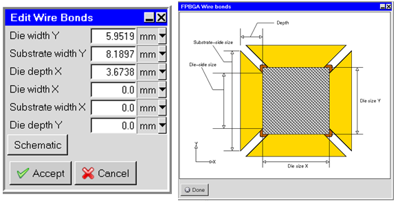
(For PBGA, cavity-down BGA, and FPBGA packages only) In the Interconnects tab, specify properties for the Wire bonds.
Click Edit wire bonds to modify wire bonds. See Figure 25.15: The Edit Wire Bonds Panel to view wire bond properties.
Specify the wire bond Material. You can change the wire bond material by selecting a material from the Material drop-down list. See Material Properties for details on material properties.
Specify the wire bond Diameter.
(For PBGA and FPBGA packages only) Specify the Average Length of the wire bonds.
(For PBGA, cavity-down BGA, and FPBGA packages only) Specify the mold Material. You can change the mold material by selecting a material from the Material drop-down list next to Mold. See Material Properties for details on material properties.
(For cavity-down BGA packages only) Specify the material for the Heat spreader. You can change the heat spreader material by selecting a material from the Material drop-down list. See Material Properties for details on material properties.
(For flip-chip and package on packages only) Specify solder bump properties.
Specify Bump diameter.
Specify Bump material. You can change bump material by selecting a material from the drop-down list.
Select Simple or Detailed for the Solder bump model.
(For flip-chip packages only) Specify whether to include an Optional heatsink by selecting Yes or No. If you select Yes, specify the properties for the heat sink.
Specify the Heatsink thickness.
Specify the Heatsink material. You can change the heat sink material by selecting a material from the Heatsink material drop-down list. See Material Properties for details on material properties.